Chinese Professional Mounting Pcb In Enclosure - Shenzhen OEM/ODM Gateway Mainboard PCB Circuit Board Manufacture 1-32 Layers Multi-layer PCB Prototype Manufacturer With Turnkey PCB Service – PhiliFast

Chinese Professional Mounting Pcb In Enclosure - Shenzhen OEM/ODM Gateway Mainboard PCB Circuit Board Manufacture 1-32 Layers Multi-layer PCB Prototype Manufacturer With Turnkey PCB Service – PhiliFast Detail:
PRODUCT SPECIFICATION:
| Base Material: | FR4-TG140 | Surface Finish: | HASL(Lead Free) |
| PCB Thickness: | 1.6mm | Solder Mask: | Green |
| PCB Size: | 96*120mm | Silkscreen: | White |
| Layer Count: | 2/L | Cu Thickness | 35um(1oz) |
| Mounting Type: | SMT+DIP | Application | Gateway |
| Testing Service | AOI,X-Ray,Function Test | Supplier type | Assembly factory |
Turnkey Sevices:
1. PCB fabrication
2. Turnkey PCBA: PCB+components+SMT and through-hole assembly+enclosure molding&housing
Main Product:
Our Advantage:
1, Programming and Functional test
2, IPC-A-610E standard, E-test, X-ray, AOI test, QC, 100% functional test.
3, Professional service. ISO SMT and through hole assembly, over 10 years experience.
4, Certification: 94v-0, CE, SGS, FCC, RoHS, ISO9001:2008, ISO14001
5, Warranty period for PCBA: 2 years.
PCBA PROCESSING CAPABILITY:
| Turnkey PCBA | PCB+components sourcing+assembly+package |
| Assembly details | SMT and Thru-hole,PCB enclosure assembly |
| Lead Time | Prototype: 10-12 working days. Mass order: 18~20 working days |
| Testing on products | Flying Probe Test,E-Testing, X-ray Inspection, AOI Test, Functional test |
| Quantity | Min quantity: 1pcs. Prototype, small order, mass order |
| Files type | PCB: Gerber files(CAM, PCB, PCBDOC) |
| Components: Bill of Materials(BOM list) | |
| Assembly: Pick&Place file, Assembly drawing | |
| PCB Panel Size | Min size: 0.25*0.25 inches(6*6mm) |
| Max size: 20*20 inches(500*500mm) | |
| PCB Solder Type | Water Soluble Solder Paste, RoHS lead free |
| Components details | Passive Down to 01005 size |
| BGA and QFN For Chip | |
| Double-sided SMT Assembly | |
| Fine Pitch to 0.8mils | |
| Part Removal and Replacement | |
| Component package | Cut Tape,Tube,Reels,Loose Parts |
PCB PROCESSING CAPABILITY:
|
1 |
Layers | 1-32 Layer |
| 2 | Board material type | FR4,Ceramic substrate board,aluminum based board, high-Tg, Rogers and more |
| 3 | Compound material lamination | 4 to 6 layers |
| 4 | Maximum dimension | 600 x 1200mm |
| 5 | Board thickness coverage | 0.2 to 6.00mm |
| 6 | Minimum line width | 3mil |
| 7 | Minimum line space | 3mil |
| 8 | Outer layer copper thickness | 8.75 to 175µm |
| 9 | Inner layer copper thickness | 17.5 to 175µm |
| 10 | Drilling hole diameter (mechanical drill) | 0.25 to 6.00mm |
| 11 | Finished hole diameter (mechanical drill) | 0.20 to 6.00mm |
| 12 | Hole diameter tolerance (mechanical drill) | 0.05mm |
| 13 | Hole position tolerance (mechanical drill) | 0.075mm |
| 14 | Laser drill hole size | 0.10mm |
| 15 | Board thickness and hole diameter ratio | 10:1 |
| 16 | Solder mask type | Green, Yellow, Black, Purple, Blue, White and Red |
| 17 | Minimum solder mask | Ø0.10mm |
| 18 | Minimum size of solder mask separation ring | 0.05mm |
| 19 | Solder mask oil plug hole diameter | 0.25 to 0.60mm |
| 20 | Impedance control tolerance | ±10% |
| 21 | Surface finish | HASL(Lead Free), ENIG, immersion silver, gold plating, immersion tin and gold finger |
Fast Delivery:
PCB In 12Hours
PCBA In 3Days
Main Products Application:
*Medical Products
* Automotive Products
* Industrial Products
* Communication Products(AVL/GPS/GSM Devices)
* Consumer Electronics.
PCB Assembly Procedures:
* Program Management
PCB Files → DCC → Program Organizing → Optimization → Checking
* SMT Management
PCB Loader → Screen Printer → Checking → SMD Placement → Checking → Air Reflow → Vision Inspection → AOI → Keeping
* PCBA Management
THT→Soldering Wave (Manual Welding) → Vision Inspection → ICT → Flash → FCT → Checking → Package → Shipment
PHILIFAST provides you the best PCB manufacture and assembly experience
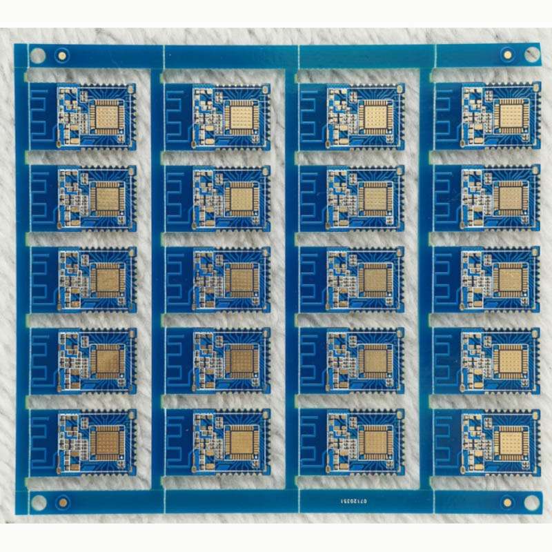
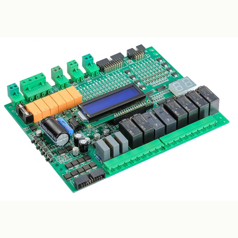
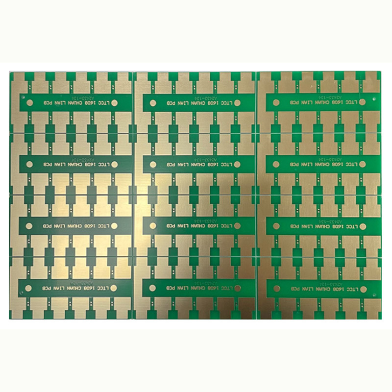
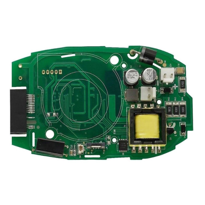
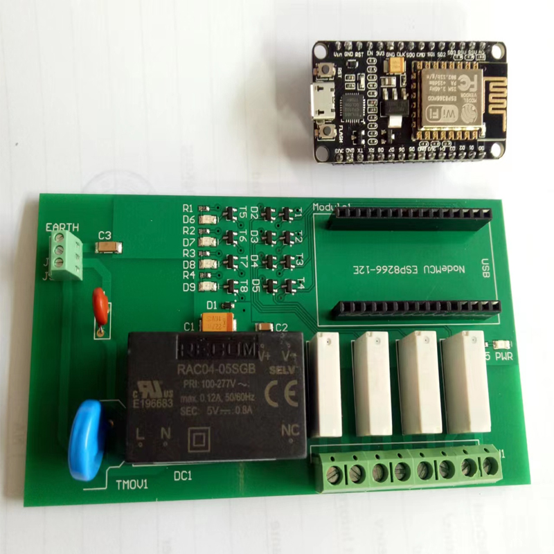
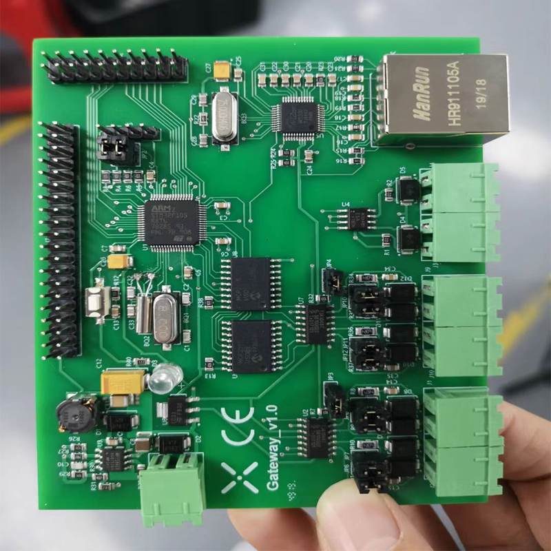
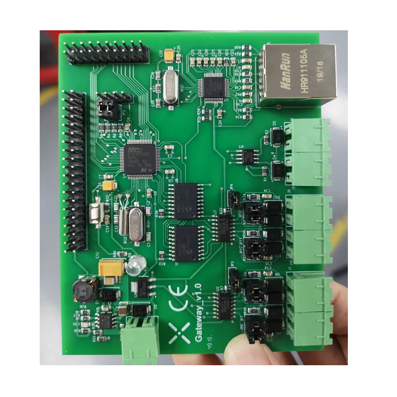
Product detail pictures:
Related Product Guide:
Our growth depends around the superior machines, exceptional talents and consistently strengthened technology forces for Chinese Professional Mounting Pcb In Enclosure - Shenzhen OEM/ODM Gateway Mainboard PCB Circuit Board Manufacture 1-32 Layers Multi-layer PCB Prototype Manufacturer With Turnkey PCB Service – PhiliFast, The product will supply to all over the world, such as: Buenos Aires, Serbia, Mauritius, With the effort to keep pace with world's trend, we will always endeavor to meet customers' demands. If you want develop any other new products, we can customize them for you. If you feel interest in any of our products or want develop new products, please feel free to contact us. We are looking forward to forming successful business relationship with customers all over the world.
The company keeps to the operation concept "scientific management, high quality and efficiency primacy, customer supreme", we have always maintained business cooperation. Work with you,we feel easy!