Navrhování DPS s vysokou hustotou propojení (HDI) vyžaduje hlubokou znalost elektrických potřeb i výrobních limitů. Technologie HDI umožňuje použít více komponent na menším prostoru. To z ní činí nejlepší volbu pro moderní elektroniku, jako jsou chytré telefony a nositelná technika.
Níže je uveden podrobný návod, jaké faktory je třeba vzít v úvahu a jak optimalizovat návrhy HDI.
Faktory, které je třeba zvážit při návrhu HDI PCB
1. Inteligentní výběr komponent
Při návrhu desky HDI se obvykle pracuje s velmi malými součástkami. Patří sem zařízení pro povrchovou montáž (SMD) a pole s kuličkovou mřížkou (BGA) s roztečí $0,65\text{ mm}$ nebo menší.
Komponenty je třeba vybírat pečlivě. Nejdůležitějším faktorem je vzdálenost mezi vývody (rozteč). Pokud jsou vývody velmi blízko u sebe, budete mít méně prostoru pro vedení měděných stop. Tato volba vám také napoví, jakou šířku stopy potřebujete a jaký typ průchodky (otvoru) musíte použít. Pokud zvolíte BGA s velmi malou roztečí, budete možná nuceni použít více vrstev nebo menší mikrodíry, abyste propojili všechny signály.
2. Používání mikrovií
Srdcem konstrukce HDI jsou mikrotrubičky. Jedná se o velmi malé otvory, obvykle o průměru menším než $0,15\text{ mm}$. Konstruktéři k vytvoření těchto otvorů často používají techniky “build-up” nebo “sekvenčního” laminování.
Mikrovíčka vám pomohou ušetřit spoustu místa. Protože jsou tak malé, vejde se jich na malou plochu více než klasických průchozích otvorů. Další velkou výhodou je jejich nízká indukčnost. Díky tomu jsou ideální pro vysokorychlostní obvody. Můžete je použít k připojení výkonových rovin k oddělovacím kondenzátorům nebo na jakémkoli místě, kde potřebujete snížit elektrický šum.
3. Výběr materiálu
Výběr správného materiálu je důležitý pro každou desku plošných spojů, ale pro HDI je ještě důležitější. Vaším cílem je najít materiál, který se snadno vyrábí, ale zároveň dobře zvládá teplo a elektřinu.
Klíčovým faktorem je fyzická tloušťka materiálu. Je třeba se podívat na “poměr stran” mikrotrhlin. Jedná se o poměr mezi hloubkou otvoru a jeho průměrem. Pokud je materiál příliš tlustý a otvor příliš malý, je velmi obtížné otvor řádně pokovit mědí. Musíte zvolit materiál, který umožňuje chemikáliím během procesu pokovování protékat otvory.
4. Přes uzávěr a offsetové mikrozásobníky
Při návrhu HDI můžete použít techniku zvanou “via-in-pad”. To znamená, že umístíte mikrovodič přímo do středu podložky pro povrchovou montáž.
Za tímto účelem je třeba průchodku “uzavřít” nebo vyplnit a následně pokovit mědí. Tím se vytvoří rovný povrch pro pájení. Při použití této metody získáte mnohem více prostoru pro vedení stop, protože průchodka nezabírá další prostor mimo podložku. Můžete také použít “odsazené” mikropropojky, kde otvory v různých vrstvách nejsou dokonale zarovnány, abyste ještě lépe hospodařili s prostorem.

5. Redukované plošné perforace
Když navrhnete napájecí a zemní rovinu pod BGA, chcete mít co nejvíce pevné mědi. Tomu se říká “Power Integrity” (PI).
V tradičních konstrukcích vytvářejí velké průchozí otvory v měděných rovinách mnoho “dutin” nebo prázdných míst. To působí jako plot, který blokuje tok proudu. V HDI jsou průchodky mnohem menší, a tak zůstává více mědi nedotčené. Tím se zlepšuje elektromagnetická kompatibilita (EMC) desky. Poskytuje také lepší stínění proti rušení.
6. Problémy se stohováním a delaminace
Uspořádání měděných a izolačních vrstev je “stack-up”. V HDI se často používají různé materiály pro různé vrstvy.
Každý materiál má “koeficient tepelné roztažnosti” (CTE). Ten udává, jak moc se materiál zvětší, když se zahřeje. Pokud mají dvě vrstvy velmi rozdílné hodnoty CTE, budou se rozpínat různou rychlostí. To může způsobit, že se vrstvy od sebe odtrhnou, což se nazývá “delaminace”. Aby se tomu předešlo, měli by se konstruktéři snažit použít pro každou vrstvu stejný materiál nebo použít materiály s velmi podobnými hodnotami CTE a mírou absorpce vlhkosti.
7. Zkušební metody
Tradiční “testování v obvodu” (ICT) není u desek HDI často možné. ICT vyžaduje velké testovací body, které zabírají příliš mnoho místa.
Místo toho konstruktéři používají funkční testování nebo metody JTAG (Joint Test Action Group). JTAG umožňuje testovat spojení mezi integrovanými obvody, aniž by bylo nutné používat fyzické testovací sondy pro každý jednotlivý vodič. Zatímco ICT je velmi dobrá při hledání konkrétních závad, JTAG je mnohem vhodnější pro husté prostředí desek HDI.
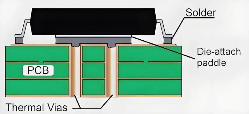
8. Řízení tepla
Desky HDI jsou velmi husté, takže se rychle zahřívají. Musíte naplánovat, jak odvádět teplo od komponent.
Měli byste se řídit IPC-2226 který stanoví pravidla pro tepelný návrh v oblasti HDI. Jednou z výhod HDI je, že dielektrické (izolační) vrstvy jsou velmi tenké. Tenké vrstvy v kombinaci s mikrovrstvami skutečně pomáhají odvádět teplo od čipů. Pokud máte velmi horkou součástku, můžete přidat “tepelné průchodky” a odvést teplo do větší měděné roviny nebo chladiče.
9. Poptávka po směrování v závislosti na kapacitě substrátu
“Potřeba trasování” je celková délka všech vodičů potřebných k propojení součástek na desce. “Kapacita substrátu” je celková délka vodičů, kterou deska skutečně pojme.
Aby byl návrh úspěšný, musí být kapacita vyšší než poptávka. Pokud je poptávka příliš vysoká, může být nutné přidat více vrstev, což však zvyšuje náklady. Návrháři se snaží tyto dvě věci vyvážit, aby návrh dokončili s co nejnižšími náklady.
10. Výpočet hustoty PWB
Složitost vašeho návrhu můžete změřit pomocí výpočtu hustoty desek s plošnými spoji (PWB). Tu měříme jako průměrnou délku stop na čtvereční palec.
Abychom to zjistili, předpokládáme, že každá “síť” (jedno elektrické spojení) má tři uzly a že každý přívod součástky je jeden uzel. Použijeme následující vzorec:
$$Wd = \beta \sqrt{Cd \times Cc}$$
Kde:
- $Wd$: Hustota PWB (průměrná délka stopy na čtvereční palec).
- $Cd$: Hustota složky (průměrný počet dílků na čtvereční palec).
- $Cc$: Složitost součástky (průměrný počet vodičů/vývodů na součástku).
- $\beta$: Konstanta podle typu obvodu.
- Použijte 2.5 pro vysoce analogové nebo diskrétní oblasti.
- Použijte 3.0 pro smíšené analogové a digitální oblasti.
- Použijte 3.5 pro čistě digitální nebo ASIC oblasti.
Tento vzorec je užitečným vodítkem. Nezapomeňte však, že každý design je jedinečný a neexistuje jediné pravidlo, které by se hodilo pro každou desku.
Jak optimalizovat návrh HDI pro elektroniku
HDI je nejrychleji rostoucí částí odvětví výroby desek plošných spojů. Díky němu jsou desky efektivnější a umožňují vyšší rychlost signálu. Ve srovnání se standardními deskami mají desky HDI mnohem tenčí linky, menší prostory a menší podložky. Hlavní rozdíl je ve způsobu propojení vrstev. Standardní desky používají otvory, které procházejí skrz, ale HDI desky používají slepé a zakopané průchodky.
Zde je několik způsobů, jak optimalizovat návrh a vyhnout se nákladným chybám.
Výběr správného typu cesty
Zvolené průchodky ovlivní výkon a cenu desky. Použití mikropropustů (slepých nebo zakopaných) může ve skutečnosti snížit celkový počet potřebných vrstev. Když máte méně vrstev, klesají náklady na materiál. Díky tomu je také výrobní proces méně složitý. Měli byste se včas poradit s výrobcem, abyste zjistili, které typy průchodek dokáže spolehlivě vyrobit.
Pečlivý výběr komponent
Při sestavování desky HDI musíte být velmi opatrní při výběru součástek. Než začnete s rozvržením, podívejte se na počet pinů a velikost součástek. Přemýšlejte o tom, jak se stopy vejdou mezi vývody. Pokud vyberete součástky, které jsou pro velikost desky příliš složité, strávíte více času návrhem a více peněz výrobou.
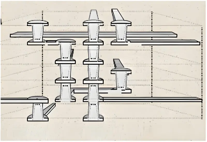
Pečlivé plánování skládky
Vrstvy na desce HDI lze uspořádat mnoha způsoby. Mezi běžné styly patří:
- 1-HDI: Jedna vrstva mikropropustů na horní a spodní straně s jádrem obsahujícím pohřbené průchodky.
- 2-HDI (bez stohování): Dvě vrstvy mikrovláken, které na sebe nedoléhají.
- Stohované 2-HDI: Mikroskopické rostliny, které sedí přímo na sobě. Mohou být vyplněny pryskyřicí nebo mědí.
Musíte si vybrat vyvážený stack-up. Pokud by sestava nebyla symetrická, mohla by se deska během zahřívání deformovat nebo ohýbat. Dobré uspořádání zlepšuje “výtěžnost” (procento vyrobených dobrých desek).
Používejte správné rozestupy
Pokud umístíte komponenty příliš blízko sebe, může dojít k elektromagnetickému rušení (EMI). K tomu dochází, když elektrické signály z jednoho vodiče pronikají do jiného vodiče. Může také vzniknout “parazitní kapacita”, která zpomaluje signály.
Součásti byste měli rozmístit tak, abyste minimalizovali namáhání a elektromagnetické rušení. Současně se ujistěte, že máte dostatek prostoru pro montáž a opravy. Pokud jsou součástky příliš blízko u sebe, je velmi obtížné je připájet nebo opravit, pokud se něco pokazí.
Zaměření na integritu signálu (SI)
Integrita signálu spočívá v zajištění čistoty elektrického signálu od jednoho konce vodiče k druhému. Abyste udrželi silné signály:
- Udržujte správný poměr stran průchodek, aby bylo měděné pokovení silné a rovnoměrné.
- Pro zkrácení délky “pahýlu” (přebytečné mědi, která visí ze stopy) použijte velmi malé mikročástice.
- Umístěte malé díly blízko sebe, aby byly signální cesty krátké.
- Rozložení zakopaných a zaslepených průchodek pro snížení fyzického namáhání materiálů desky.
Použití pokročilých nástrojů pro navrhování
Návrh desky plošných spojů HDI je pro základní software příliš náročný. Výrobci a konstruktéři potřebují profesionální software CAD (Computer-Aided Design) a CAM (Computer-Aided Manufacturing). Používají také technologii “Laser Direct Imaging” (LDI) pro kreslení drobných čar na desce. Protože jsou tolerance tak malé, jsou zkušenosti obsluhy stejně důležité jako stroje.
Výhody napříč odvětvími
Desky HDI se používají, protože díky nim elektronika funguje lépe. Najdete je v:
- Počítače: Pro rychlejší zpracování dat.
- Chytré telefony: Vměstnat více funkcí do zařízení kapesní velikosti.
- Zdravotnické prostředky: Zmenšit vybavení pro lékaře a zvýšit jeho přenosnost.
Úspěch vašeho projektu HDI závisí na tom, jak dobře naplánujete rozložení a jak dobře budete spolupracovat s výrobcem. Dodržováním těchto tipů můžete vytvořit vysoce výkonnou desku, která bude spolehlivá a cenově výhodná.