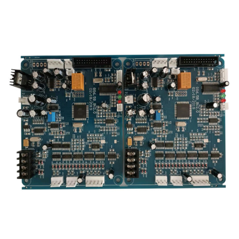
Custom Electronic Circuit Board Turnkey Service Multilayer Pcba Assembly Pcb SMD BGA Mounting With AOI/X-ray Inspection
PRODUCT SPECIFICATION:
| Base Material: | FR4-TG140 | Surface Finish: | HASL(Lead Free) |
| PCB Thickness: | 1.6mm | Solder Mask: | Blue |
| PCB Size: | 90*160mm | Silkscreen: | White |
| Layer Count: | 2/L | Cu Thickness | 35um(1oz) |
| Mounting Type: | SMT+DIP | SMT Package | 0201,BGA, QFN |
| Testing Service | AOI,X-Ray,Function Test | Supplier type | Assembly factory |
Turnkey Sevices:
1. PCB fabrication
2. Turnkey PCBA: PCB+components+SMT and through-hole assembly+enclosure molding&housing
Main Product:
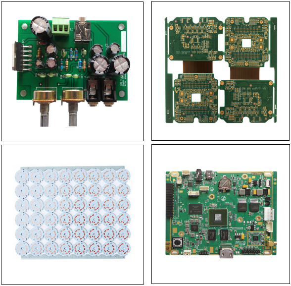
Our Advantage:
1, Programming and Functional test
2, IPC-A-610E standard, E-test, X-ray, AOI test, QC, 100% functional test.
3, Professional service. ISO SMT and through hole assembly, over 10 years experience.
4, Certification: 94v-0, CE, SGS, FCC, RoHS, ISO9001:2008, ISO14001
5, Warranty period for PCBA: 2 years.
PCBA PROCESSING CAPABILITY:
| Turnkey PCBA | PCB+components sourcing+assembly+package |
| Assembly details | SMT and Thru-hole,PCB enclosure assembly |
| Lead Time | Prototype: 10-12 working days. Mass order: 18~20 working days |
| Testing on products | Flying Probe Test,E-Testing, X-ray Inspection, AOI Test, Functional test |
| Quantity | Min quantity: 1pcs. Prototype, small order, mass order |
| Files type | PCB: Gerber files(CAM, PCB, PCBDOC) |
| Components: Bill of Materials(BOM list) | |
| Assembly: Pick&Place file, Assembly drawing | |
| PCB Panel Size | Min size: 0.25*0.25 inches(6*6mm) |
| Max size: 20*20 inches(500*500mm) | |
| PCB Solder Type | Water Soluble Solder Paste, RoHS lead free |
| Components details | Passive Down to 01005 size |
| BGA and QFN For Chip | |
| Double-sided SMT Assembly | |
| Fine Pitch to 0.8mils | |
| Part Removal and Replacement | |
| Component package | Cut Tape,Tube,Reels,Loose Parts |
PCB PROCESSING CAPABILITY:
|
1 |
Layers | 1-32 Layer |
| 2 | Board material type | FR4,Ceramic substrate board,aluminum based board, high-Tg, Rogers and more |
| 3 | Compound material lamination | 4 to 6 layers |
| 4 | Maximum dimension | 600 x 1200mm |
| 5 | Board thickness coverage | 0.2 to 6.00mm |
| 6 | Minimum line width | 3mil |
| 7 | Minimum line space | 3mil |
| 8 | Outer layer copper thickness | 8.75 to 175µm |
| 9 | Inner layer copper thickness | 17.5 to 175µm |
| 10 | Drilling hole diameter (mechanical drill) | 0.25 to 6.00mm |
| 11 | Finished hole diameter (mechanical drill) | 0.20 to 6.00mm |
| 12 | Hole diameter tolerance (mechanical drill) | 0.05mm |
| 13 | Hole position tolerance (mechanical drill) | 0.075mm |
| 14 | Laser drill hole size | 0.10mm |
| 15 | Board thickness and hole diameter ratio | 10:1 |
| 16 | Solder mask type | Green, Yellow, Black, Purple, Blue, White and Red |
| 17 | Minimum solder mask | Ø0.10mm |
| 18 | Minimum size of solder mask separation ring | 0.05mm |
| 19 | Solder mask oil plug hole diameter | 0.25 to 0.60mm |
| 20 | Impedance control tolerance | ±10% |
| 21 | Surface finish | HASL(Lead Free), ENIG, immersion silver, gold plating, immersion tin and gold finger |
Fast Delivery:
PCB In 12Hours
PCBA In 3Days
Main Products Application:
*Medical Products
* Automotive Products
* Industrial Products
* Communication Products(AVL/GPS/GSM Devices)
* Consumer Electronics.
PCB Assembly Procedures:
* Program Management
PCB Files → DCC → Program Organizing → Optimization → Checking
* SMT Management
PCB Loader → Screen Printer → Checking → SMD Placement → Checking → Air Reflow → Vision Inspection → AOI → Keeping
* PCBA Management
THT→Soldering Wave (Manual Welding) → Vision Inspection → ICT → Flash → FCT → Checking → Package → Shipment
PHILIFAST provides you the best PCB manufacture and assembly experience


