


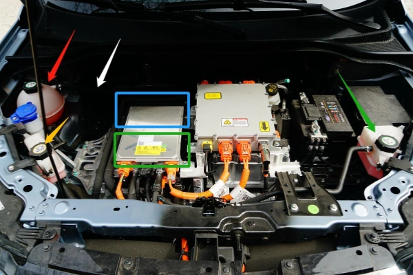
With the rapid development of battery performance and Intelligent driving technology, EV charger tailored solutions need to improve their performance to meet the specific charging requirements,especially in assembling of those customized EV charger PCB boards.
How to make the best assembly process and solution for EV charger PCB?
1. Optimizing the Design of EV Charger PCB
The best solution for PCB assembly is to optimize the design of the PCB itself:
1.1 PCB Layout
Consider to design your EV charger PCB with high-power components (e.g., power MOSFETs, rectifiers, capacitors) in positions that contribute to better heat dissipation. Considering reducing the risk of interference for those function components e.g., power components, control components during PCB-layout
1.2 Thermal Management
EV charger main board will generate substantial heat during high-power charging. Poor thermal dissipation leads overheating and reduce the use lifespan of both the charger and the vehicle battery.Thermal vias and wider power trace design is also a good way to take heat away from power components. In addition,Heavy Copper circuit PCB design around high-power components can help dissipate heat more effectively,normally the copper thickness for EV charger PCB is 2oz,3oz . Except that, copper bar soldering,heat sinks or cooling fans contribute a lot for thermal dissipation
2. The Necessity Of Design for Manufacturing (DFM) Before PCB Assembly
2.1 Design Rule Checks (DRC)
In order to improve Manufacturability and yield,the engineer need to check final design files before production to ensure the PCB layout adheres to processing rules of the manufacturer. These rules can avoid some issues during fabrication and assembly. DRC checks mainly includes trace width and spacing,via and pad size and the spacer among pads
- Trace width and spacing: tiny trace width and spacing may lead short circuits or signal interference.we have to consider the minimum trace width and spacing
- Pads and vias: Pads and vias must meet your PCB manufacturer’s drill and annular ring tolerances. Undersized annular rings or pads can lead to broken connections, plated-through defects, or higher fabrication costs.
- Pad-to-pad spacing: we need to ensure sufficient spacer among pads to avoid solder bridging during assembly.short cut may be caused if the spacer is tiny.
- Component clearances: It’s also very important to ensuring enough clearance between components for soldering and to avoid mechanical interference.
2.2 Component Placement Optimization
Component placement is critical to improve high-efficient assembly, good performance, and manufacturability:
- Component layout: to improve the efficiency and lower labor costs,all components need to be placed efficiently by machines (e.g., pick-and-place machines).manual placement is hard to place all components in a right way and waste lots of time,so we need to consider PCB layout of components
- Clarify component orientation and polarity clearly: For those components with orientation and polarity should be oriented correctly to avoid rework and repairing during assembly.
2.3 PCB Panelization for Efficient Manufacturing
DFM engineer can arrange multiple boards on a single panel to optimize the PCB fabrication and assembly process. Especially for those small size PCB boards.In order to reduce waste.considering the design of v-groove cuts, mouse bites, or breakaway tabs for easy separation after assembly.
3. Customer Case Sharing: Providing the Best Assembly Solution for Charging Pile PCB
Because of the customer’s trust in us, we received a PCB order from an European client for the production and assembly of 1,500 sets of EV charging main and sub PCB boards.
3.1 Design
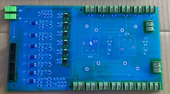
The PCBs use a 4-layer layout with 2 oz copper thickness and resin-filled via process. The boards are relatively large and include nearly 200 component types, totaling thousands of electronic parts.
3.2 PCB Manufacturing
Before PCB production, our engineering team rechecked the Gerber files, including Top/Bottom layers, Silkscreen, Solder Mask, Drill Data, Mechanical Layer and other key files. They also verified the file format (e.g., RS-274X) to ensure it meets production requirements and prevent data parsing failures due to format errors. Engineers used professional software such as CAM350 and Altium Designer to perform comprehensive DRC checks on the Gerber files according to internal production standards and customer requirements. The checks mainly include hole size accuracy, spacing and trace width, pad integrity, silkscreen accuracy, and special processes. For special process requirements in the customer’s design (such as blind/buried vias, thick copper, impedance control), engineers focused on verifying that the design parameters match production capabilities and optimized and generated an EQ (Engineering Qualification) file. After internal review approval of the EQ file, it’s converted into Gerber and drill files ready for production, and a BOM (bill of materials) and assembly drawings were produced. Production files must be exactly consistent with the EQ file and marked with version number and effective date.
3.3 Components Procurement
During PCB production,our professional purchase department order BOM components one by one as per the final BOM which our engineer checked and confirmed with the customer.
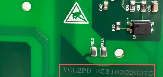
3.4 Laser Marking of Serial Number On PCBs
Before all components mount on the board,we need to make series number on PCBs by laser marking.firstly we got alphanumeric serial number (e.g., SN00001) or format,Placement and Size & font from customer,each boards has a specific serial number marked by laser to identify
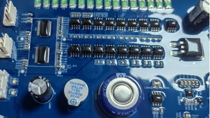
3.5 Assembly of EV Charger PCB
Assembly of EV charger main and sub PCBs including SMT assembly, THT assembly, we go through wave soldering, dry icing blasting,conformal coating, functional test, and final inspection.
Conclusion
Assembling EV charger PCBs is not fundamentally different from other PCB assemblies. EV charger PCBs meet higher safety, reliability, and regulatory demands compared with typical consumer boards,for this type of industrial-control PCB we must pay extra attention to many more details
- High-voltage & isolation
- Thermal management
- Robustness & longevity
- Power handling & current paths
- EMC/EMI control
- Safety-critical components & redundancy
- Process controls & qualification
- Traceability & serialization
- Environmental & reliability testing
- Field serviceability & documentation
- Handling & safety in production
- Supplier & component selection

