


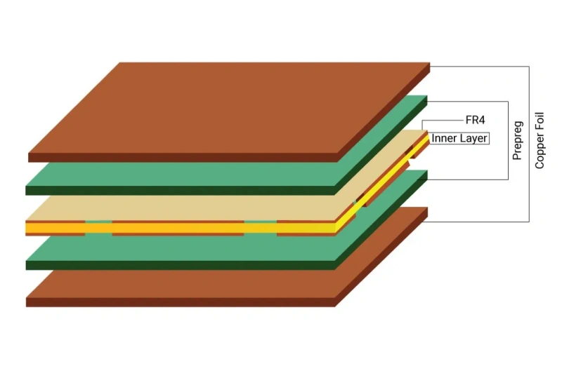
1. Hvad er kobberfolie?
Kobberfolie er en tynd, kontinuerlig metalplade. Det er et elektroaflejret materiale af negativ type. Folien placeres på bunden af printkortet. Den fungerer som leder på printet. Det binder godt til isolerende lag. Det tager loddemaske og andre beskyttende lag. Efter ætsning danner det resterende kobber kredsløbsmønsteret. I den tidlige produktion brugte man rullet kobberfolie. Det betyder, at kobberblokke er fladet ud til tynde plader.
Hvor tyk er kobberfolien på et printkort?
2. Enhed for kobbertykkelse: oz
PCB-kobbertykkelse angives normalt i oz (ounce). Ounce er en vægtenhed. Forholdet mellem ounce og gram er:
1 oz ≈ 28,35 g.
I printkortindustrien betyder 1 oz vægten af 1 oz kobber fordelt jævnt over 1 kvadratfod (ft²). Det jævne lag har en vis tykkelse. Den tykkelse er ca. 35 μm. Ved hjælp af en formel:
1 oz = 28,35 g / ft².
Nedenfor viser jeg beregningen trin for trin, så resultatet er tydeligt:
- Tag 1 oz masse: 28,35 g.
- Kobberets massefylde: 8,93 g/cm³.
- 1 ft² = 929,03 cm².
Tykkelse i cm = masse / (massefylde × areal)
= 28,35 / (8,93 × 929,03) cm
= 28,35 / 82973,558 ≈ 0,00341721 cm.
Omregn til mikrometer (μm): 0,00341721 cm = 0,00341721 × 10.000 μm = 34,17 μm.
Så 1 oz kobberfolie ≈ 34,17 μm. Denne værdi afrundes normalt og angives som 35 μm. I britiske enheder er 34,17 μm = 0,03417 mm. En mil = 0,0254 mm, så tykkelsen ≈ 1,345 mil. Folk siger ofte 1 oz ≈ 35 μm ≈ 1,35 mil.
3. Almindelige værdier for kobbertykkelse
Almindelige værdier for kobbertykkelse, der bruges i PCB'er, er:
- 0,5 oz ≈ 17,5 μm
- 1 oz ≈ 35 μm
- 2 oz ≈ 70 μm
- 3 oz ≈ 105 μm
Typiske enkelt- og dobbeltsidede printkort Brug om 35 μm (1 oz) kobber. Nogle kort bruger 50 μm eller 70 μm også kobber. Ved flerlagsplader er de yderste lag ofte 35 μm (1 oz). De indre lag er ofte 17,5 μm (0,5 oz).
Tykke kobberplader starter ved ca. 3 oz og derover. Disse kort bruges i højstrøms- eller højspændingsprodukter, f.eks. strømforsyninger.
4. Strømføringsevne for forskellige kobbertykkelser
Nedenfor er en praktisk tabel, der viser typisk strømkapacitet for kobberstrimler af forskellig tykkelse og bredde. Tabellen viser strømstyrke (A) og nødvendig bredde (mm) for kobbertykkelser på 70 μm, 50 μm, og 35 μm. Testtykkelsesparameteren i tabellen er t = 10 (dette er en eksempelreferenceværdi, der bruges i kildetabellen).
Bemærk: Når du bruger kobberfolie som leder for høj strøm, er det almindeligt at reducere tabelværdierne med 50% for et sikkert valg. Det betyder, at du skal vælge en bredde, der svarer til ca. halvdelen af den angivne strøm, hvis du vil have en sikkerhedsmargin.
| Strøm (A) / Bredde (mm) for 70 μm | Strøm (A) / Bredde (mm) for 50 μm | Strøm (A) / Bredde (mm) for 35 μm |
|---|---|---|
| 6,00 A - 2,50 mm | 5,10 A - 2,50 mm | 4,50 A - 2,50 mm |
| 5,10 A - 2,00 mm | 4,30 A - 2,00 mm | 4,00 A - 2,00 mm |
| 4,20 A - 1,50 mm | 3,50 A - 1,50 mm | 3,20 A - 1,50 mm |
| 3,60 A - 1,20 mm | 3,00 A - 1,20 mm | 2,70 A - 1,20 mm |
| 3,20 A - 1,00 mm | 2,60 A - 1,00 mm | 2,30 A - 1,00 mm |
| 2,80 A - 0,80 mm | 2,40 A - 0,80 mm | 2,00 A - 0,80 mm |
| 2,30 A - 0,60 mm | 1,90 A - 0,60 mm | 1,60 A - 0,60 mm |
| 2,00 A - 0,50 mm | 1,70 A - 0,50 mm | 1,35 A - 0,50 mm |
| 1,70 A - 0,40 mm | 1,35 A - 0,40 mm | 1,10 A - 0,40 mm |
| 1,30 A - 0,30 mm | 1,10 A - 0,30 mm | 0,80 A - 0,30 mm |
| 0,90 A - 0,20 mm | 0,70 A - 0,20 mm | 0,55 A - 0,20 mm |
| 0,70 A - 0,15 mm | 0,50 A - 0,15 mm | 0,20 A - 0,15 mm |
Igen skal du vælge en sikker margin. En almindelig regel er at reducere disse tabelværdier med 50%, når du designer til produktion.
5. Andre praktiske bemærkninger om kobber som leder
- Hvis du bruger kobberfolie som en lang strimmelleder, skal du tjekke dens strømkapacitet. Tag for eksempel en typisk tykkelse på 0,03 mm (30 μm). Hvis kobberstrimlen har bredden W (mm) og længden L (mm), kan DC-modstanden tilnærmes ved: R ≈ 0,0005 × L / W (ohm) Denne formel giver et hurtigt estimat til designkontrol.
- Kobberets strømkapacitet afhænger også af delene på kortet, antal og typer af dele og køling. Så den reelle strømkapacitet afhænger af både kobbergeometri og termiske forhold.
- En praktisk tommelfingerregel er: Strømkapacitet ≈ 0,15 × W (A). Dette er et empirisk estimat, der bruges i nogle tilfælde. Det er enkelt og konservativt for mange tavler.
6. Eksempel: areal og strømtæthed
Tag et almindeligt tilfælde: kobbertykkelse 35 μm og sporbredde 1 mm. Tværsnitsarealet er:
- Areal = tykkelse × bredde = 0,035 mm × 1 mm = 0,035 mm².
Hvis du bruger en regel om strømtæthed på 30 A/mm², så er strømmen pr. 1 mm bredde ≈ 30 × 0,035 = 1,05 A. Så ca. 1 A pr. mm sporbredde ifølge denne tommelfingerregel.
7. IPC-formler for mere præcis strøm og temperaturstigning
IPC-2152 og IPC-D-275 giver mere nøjagtige modeller. Teksten indeholder IPC-D-275-formler i en fælles form:
- For interne spor: I = 0,0150 × (ΔT^0,5453) × (A^0,7349)
- For eksterne spor: I = 0,0647 × (ΔT^0,4281) × (A^0,6732)
I disse formler:
- I er strømstyrken i ampere.
- ΔT er den tilladte temperaturstigning i °C.
- A er tværsnitsarealet i mil² (eller andre enheder afhængigt af, hvordan du anvender formlen). Brug ensartede enheder, når du anvender formlerne.
Brug IPC-metoder, hvis du har brug for nøjagtig tilladt strøm for en given temperaturstigning.
8. Kobbertykkelse og dielektrisk tilpasning
I printkortdesign betyder “kobbertykkelse - dielektrisk matchning”, at du vælger kobbertykkelse og kortets dielektrikum sammen. Dette er for at opfylde elektriske behov, termiske behov og mekaniske behov. Vigtige punkter:
8.1 Kobbervægt (kobbertykkelse)
- Enhed: oz/ft² (f.eks. 0,5 oz, 1 oz, 2 oz, 3 oz).
- 1 oz ≈ 35 μm ≈ 1,35 mil.
- Effekter:
- Strømførende: Tykkere kobber fører mere strøm.
- Tab: Ved høje frekvenser er skin-effekten vigtig. Tykkere kobber kan i nogle tilfælde reducere ledertabet.
- Termisk: Tykkere kobber hjælper med at sprede varmen.
- Ætsning: Tykkere kobber gør fint ætsningsarbejde sværere. Mindste sporbredde og -afstand kan øges.
- Omkostninger: Tykkere kobber koster mere.
8.2 Dielektrisk materiale
Vigtige dielektriske egenskaber:
- Dielektrisk konstant (Dk eller εr): påvirker signalets hastighed og impedans.
- Tabstangent (Df): påvirker højfrekvenstab.
- Tykkelse (H): Med kobbertykkelse bestemmer H impedans og kapacitans.
- CTE og Tg: termisk pålidelighed.
Almindelige materialer: fr4 til almindelig brug, høj-Tg fr4 og specielle højfrekvente materialer (f.eks. Rogers).
8.3 Regler for matchning
- For impedansstyring er en almindelig mikrostrip-formel: Z0 ≈ (87 / sqrt(εr_eff + 1,41)) * ln(5,98H / (0,8W + T)), hvor Z0 er impedans, εr_eff er effektiv dielektrisk konstant, H er dielektrisk tykkelse, W er sporbredde, T er kobbertykkelse.
- Hvis kobbertykkelsen øges, falder impedansen for samme bredde og dielektrikum. Så du skal øge bredden eller øge den dielektriske tykkelse for at bevare den samme impedans.
- For højfrekvente signaler er skin depth vigtig. Kobbertykkelsen skal være mindst flere gange huddybden ved den højeste frekvens af interesse. Ved meget høje frekvenser betyder overfladeruhed også noget. Brug kobber med lav ruhed, hvis du har brug for lavt tab.
- Brug tykkere kobber (≥ 2 oz) til strømforsyninger og kraftig strøm, og overvej termisk ledende dielektrikum eller metalkerneplader til varmestyring.
8.4 Fremstillingsmuligheder
- Tykt kobber (≥ 3 oz) kræver større spor/afstandsregler for at undgå ætsningsproblemer.
- Tynde dielektrika kræver nøje kontrol over kobbertykkelsen. Variationer påvirker impedansen.
9. Udvælgelsestabel (kort vejledning)
| Anvendelsesscenarie | Anbefalet kobbervægt | Anbefalet dielektrisk materiale | Matchende årsag |
|---|---|---|---|
| Digital højhastighed (>5 Gbps) | 0,5 oz - 1 oz | lav-Df FR4 /. Rogers RO4000 | Fin routing, lavt tab, lettere impedansstyring. |
| Effektmoduler / høj strøm | 2 oz - 6 oz+ | FR4 Materialer med høj Tg / høj varmeledningsevne | Højere strømkapacitet og bedre varmeafledning. |
| RF/mikrobølge (>10 GHz) | 0,5 oz (lav ruhed) | Rogers RO3000 / Teflon (PTFE) | Ultra-lavt tab og optimerede overfladeeffekter til RF. |
| Generel forbrugerelektronik | 1 oz | standard FR4 | Afbalancerede omkostninger og en moden proces. |
| HDI-kort med høj densitet | 0,5 oz - 1 oz | FR4 Høj-Tg/lav-CTE-materialer | Fine spor og pålidelig laser via performance. |
10. Praktiske råd
- Angiv først dine behov: strøm, signalhastighed, impedans, varme.
- Planlæg stackup med de rigtige værktøjer.
- Lav impedanssimulering med materiale Dk og kobbertykkelse.
- Spørg kortproducenten om tolerancer for kobbertykkelse og dielektriske muligheder.
- I højfrekvente tilfælde skal du måle materiale Dk og Df, hvis det er muligt.
Bemærk: Den nominelle kobbervægt (f.eks. 1 oz) er starttykkelsen før ætsning. Efter ætsning kan sporet have tilspidsede sider. Til reelle impedanskontroller skal du bruge enten gennemsnitstykkelse eller board house-vejledning.

