Factory Promotional Printed Circuit Board Assembly Services - Shenzhen OEM/ODM Gateway Mainboard PCB Circuit Board Manufacture 1-32 Layers Multi-layer PCB Prototype Manufacturer With Turnkey PCB Service – PhiliFast

Factory Promotional Printed Circuit Board Assembly Services - Shenzhen OEM/ODM Gateway Mainboard PCB Circuit Board Manufacture 1-32 Layers Multi-layer PCB Prototype Manufacturer With Turnkey PCB Service – PhiliFast Detail:
PRODUCT SPECIFICATION:
| Base Material: | FR4-TG140 | Surface Finish: | HASL(Lead Free) |
| PCB Thickness: | 1.6mm | Solder Mask: | Green |
| PCB Size: | 96*120mm | Silkscreen: | White |
| Layer Count: | 2/L | Cu Thickness | 35um(1oz) |
| Mounting Type: | SMT+DIP | Application | Gateway |
| Testing Service | AOI,X-Ray,Function Test | Supplier type | Assembly factory |
Turnkey Sevices:
1. PCB fabrication
2. Turnkey PCBA: PCB+components+SMT and through-hole assembly+enclosure molding&housing
Main Product:
Our Advantage:
1, Programming and Functional test
2, IPC-A-610E standard, E-test, X-ray, AOI test, QC, 100% functional test.
3, Professional service. ISO SMT and through hole assembly, over 10 years experience.
4, Certification: 94v-0, CE, SGS, FCC, RoHS, ISO9001:2008, ISO14001
5, Warranty period for PCBA: 2 years.
PCBA PROCESSING CAPABILITY:
| Turnkey PCBA | PCB+components sourcing+assembly+package |
| Assembly details | SMT and Thru-hole,PCB enclosure assembly |
| Lead Time | Prototype: 10-12 working days. Mass order: 18~20 working days |
| Testing on products | Flying Probe Test,E-Testing, X-ray Inspection, AOI Test, Functional test |
| Quantity | Min quantity: 1pcs. Prototype, small order, mass order |
| Files type | PCB: Gerber files(CAM, PCB, PCBDOC) |
| Components: Bill of Materials(BOM list) | |
| Assembly: Pick&Place file, Assembly drawing | |
| PCB Panel Size | Min size: 0.25*0.25 inches(6*6mm) |
| Max size: 20*20 inches(500*500mm) | |
| PCB Solder Type | Water Soluble Solder Paste, RoHS lead free |
| Components details | Passive Down to 01005 size |
| BGA and QFN For Chip | |
| Double-sided SMT Assembly | |
| Fine Pitch to 0.8mils | |
| Part Removal and Replacement | |
| Component package | Cut Tape,Tube,Reels,Loose Parts |
PCB PROCESSING CAPABILITY:
|
1 |
Layers | 1-32 Layer |
| 2 | Board material type | FR4,Ceramic substrate board,aluminum based board, high-Tg, Rogers and more |
| 3 | Compound material lamination | 4 to 6 layers |
| 4 | Maximum dimension | 600 x 1200mm |
| 5 | Board thickness coverage | 0.2 to 6.00mm |
| 6 | Minimum line width | 3mil |
| 7 | Minimum line space | 3mil |
| 8 | Outer layer copper thickness | 8.75 to 175µm |
| 9 | Inner layer copper thickness | 17.5 to 175µm |
| 10 | Drilling hole diameter (mechanical drill) | 0.25 to 6.00mm |
| 11 | Finished hole diameter (mechanical drill) | 0.20 to 6.00mm |
| 12 | Hole diameter tolerance (mechanical drill) | 0.05mm |
| 13 | Hole position tolerance (mechanical drill) | 0.075mm |
| 14 | Laser drill hole size | 0.10mm |
| 15 | Board thickness and hole diameter ratio | 10:1 |
| 16 | Solder mask type | Green, Yellow, Black, Purple, Blue, White and Red |
| 17 | Minimum solder mask | Ø0.10mm |
| 18 | Minimum size of solder mask separation ring | 0.05mm |
| 19 | Solder mask oil plug hole diameter | 0.25 to 0.60mm |
| 20 | Impedance control tolerance | ±10% |
| 21 | Surface finish | HASL(Lead Free), ENIG, immersion silver, gold plating, immersion tin and gold finger |
Fast Delivery:
PCB In 12Hours
PCBA In 3Days
Main Products Application:
*Medical Products
* Automotive Products
* Industrial Products
* Communication Products(AVL/GPS/GSM Devices)
* Consumer Electronics.
PCB Assembly Procedures:
* Program Management
PCB Files → DCC → Program Organizing → Optimization → Checking
* SMT Management
PCB Loader → Screen Printer → Checking → SMD Placement → Checking → Air Reflow → Vision Inspection → AOI → Keeping
* PCBA Management
THT→Soldering Wave (Manual Welding) → Vision Inspection → ICT → Flash → FCT → Checking → Package → Shipment
PHILIFAST provides you the best PCB manufacture and assembly experience
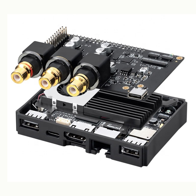
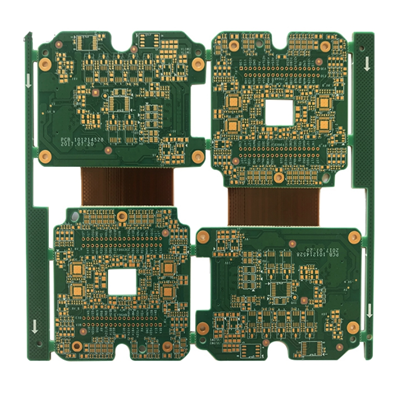
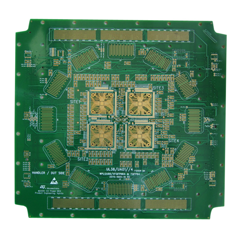
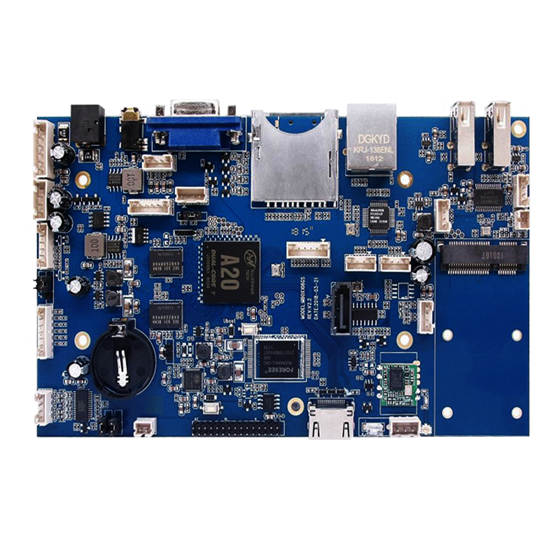
Product detail pictures:
Related Product Guide:
To create extra value for customers is our enterprise philosophy; buyer growing is our working chase for Factory Promotional Printed Circuit Board Assembly Services - Shenzhen OEM/ODM Gateway Mainboard PCB Circuit Board Manufacture 1-32 Layers Multi-layer PCB Prototype Manufacturer With Turnkey PCB Service – PhiliFast, The product will supply to all over the world, such as: San Diego, Sevilla, Bangladesh, Really should any of these items be of interest to you, please let us know. We will be pleased to give you a quotation upon receipt of one's detailed specifications. We've our personal specialist R&D enginners to meet any of the requriements, We look forward to receiving your enquires soon and hope to have the chance to work together with you inside the future. Welcome to take a look at our organization.
The sales manager has a good English level and skilled professional knowledge, we have a good communication. He is a warm and cheerful man, we have a pleasant cooperation and we became very good friends in private.