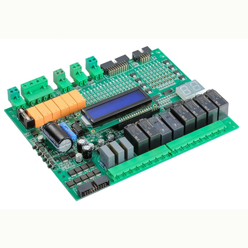
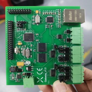
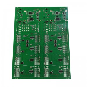
Shenzhen Fast- Speed Turnkey PCB Assembly Electronics Circuit Board Manufacturing With Professional Engineering Servicee
PRODUCT SPECIFICATION:
| Base Material: | FR4-TG140 | Surface Finish: | HASL(LF) |
| PCB Thickness: | 1.6mm | Solder Mask: | Green |
| PCB Size: | 72*120mm | Silkscreen: | White |
| Layer Count: | 2/L | Cu Thickness | 35um(1oz) |
Why us:
1. We have been engaged in electronic processing for more than ten years, with rich experience in the industry.
2. With the only professional qualification in the industry- high- speed PCB design special ability.
3. Can be pasted IC/ BGA, minimum IC foot distance 0.25mm BGA ball distance up to 0.25mm.
4. Our flexible production, superior equipment performance, can undertake almost all product projects.
We are confident that our products will make a complement for your business and improve your values to the biggest.
| PCB Base material: | FR4, Rogers, Aluminium,Copper-base, PI, PET |
| Layer: | 1-32 layer |
| PCB Thickness: | 0.4-3.0mm |
| Copper thickness: | 0.5-3OZ |
| Solder mask: | green, red, blue, yellow, black, white, purple etc |
| Min. line width | 3mil |
| Min. line space: | 3mil |
| Min. hole diameter: | 0.25mm |
| Max board size : | 600 x 1200mm |
|
Surface Finish: |
HALS/ HALS lead free/ Chemical tin/ Chemical Gold/ Immersion gold/ Immersion Silver Gold/ Osp/ Gold Plating, etc |
| Certificate | UL, ISO9001, ISO14001, ROHS, |
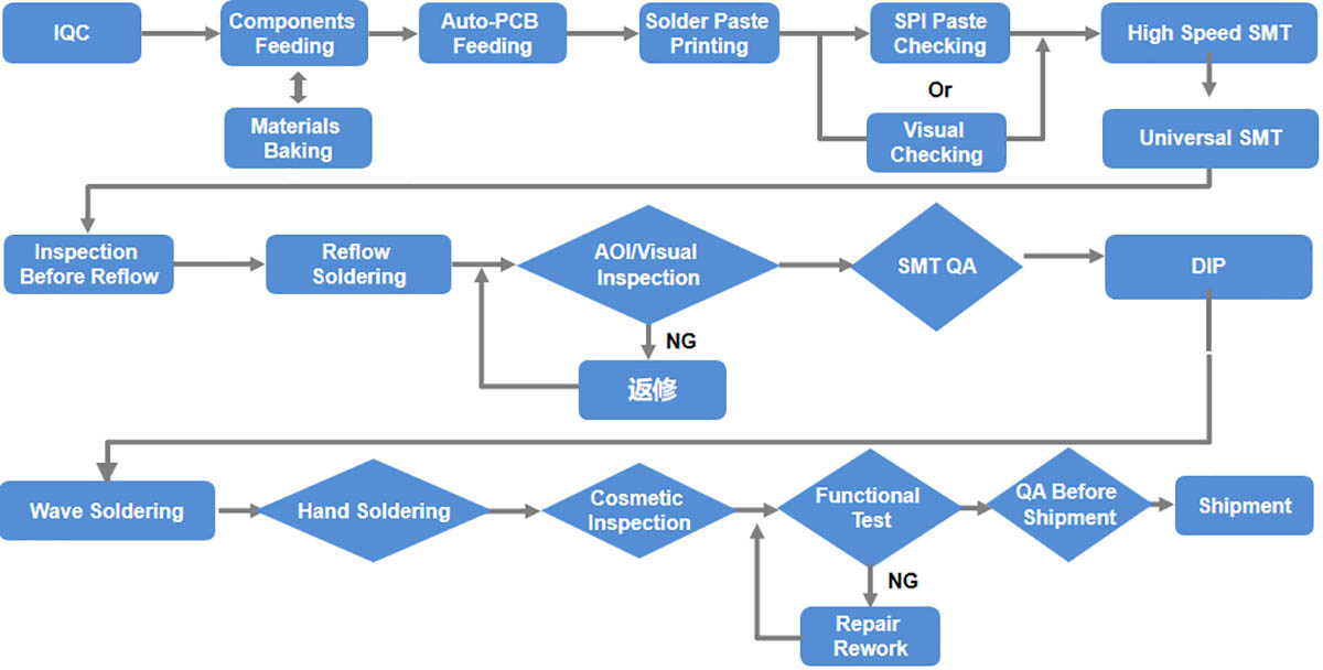
PCB Assembly Process:
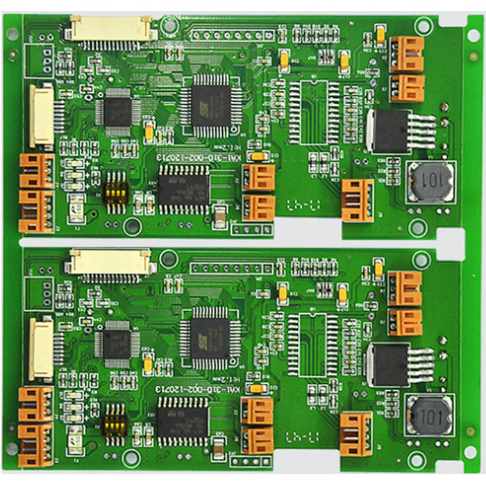
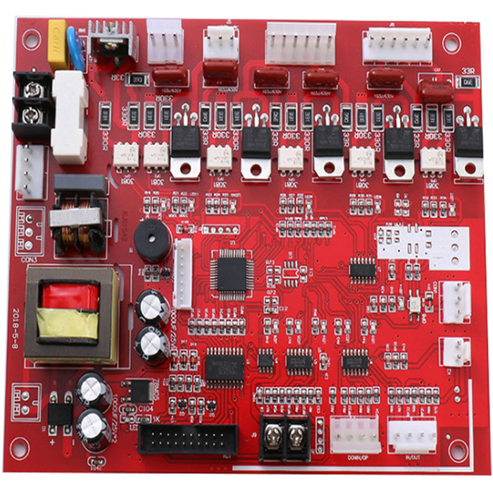
Main Product:
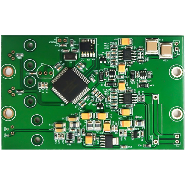
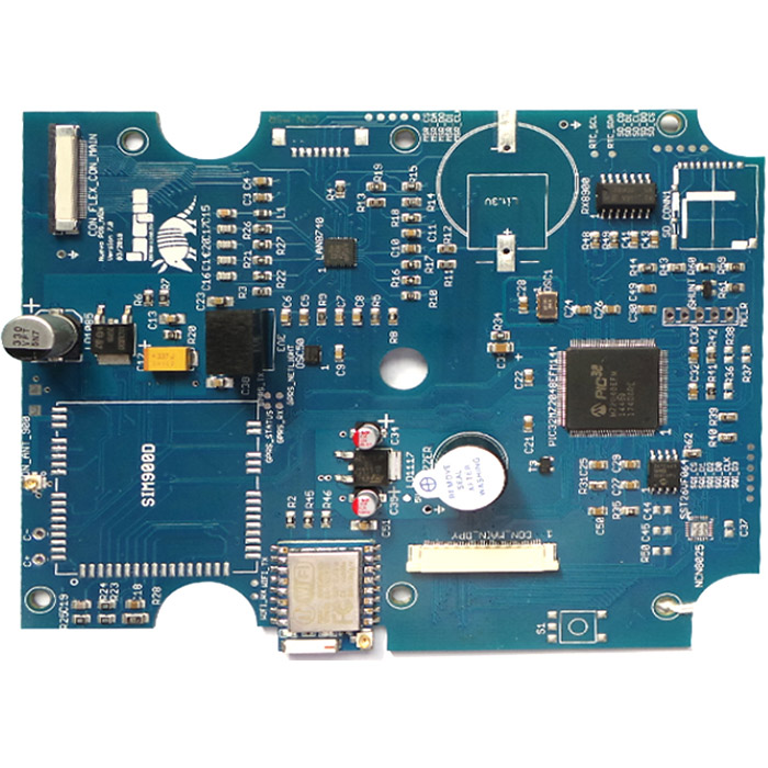
How we control the quality:
1. Process review:
1.1 Confirm customer special requirements and product special characteristics (the mountability and temperature resistance of structural special-shaped parts)
1.2 Confirm whether the BOM and PCB manufacturing data are up to date, whether there are any items to be confirmed, etc.
1.3 Assess whether the PCB shape (joint board structure) process can be mass-produced.
1.4 Manufacturability evaluation of special pad process of PCB board (gold, OSP, spray tin, SMD, NSMD, etc.).
1.5 Design different opening methods and choose different mesh steel sheets for different process PCBs.
1.6 Verification and evaluation of the suitability of special-shaped parts and other special parts with PCB pads.
2. Incoming inspection (IQC)
Inspection purpose: to prevent poor manufacturing process due to poor materials and unqualified quality of refurbished materials on the line to prevent aging loss.
3. Material classification management:
Manage materials and manage materials by classification.
4. SPI Solder Paste Inspection
Inspection purpose: find the defective solder paste printing in advance to avoid flowing into the next process.
5. AOI Inspection
Inspection purpose: to check whether the produced products have errors, omissions, and bad materials flowing out of the next process.
6. SMT First Article Inspection
Test purpose: to confirm the correctness of the production line placement process, to ensure that the parameters of each RC component are within the standard range.
7. IPQC product inspection:
Inspection purpose: to conduct random inspections of all production processes and whether they are consistent with the work instructions.
8. Visual inspection
Inspection purpose: according to the IPC610D standard, inspect the surface- mounted PCBA that has been soldered for errors, omissions, and virtual connections.
9. X- Ray Welding inspection
Inspection purpose: to inspect the solder joints of the original invisible to the naked eye to ensure the reliability of each solder ball of the BGA.
10. QC Manual inspection
According to the standard IPC- 610 inspection standard, the finished boards are inspected, and 99.98% of good products are guaranteed to be shipped.
11. QA Shipment inspection
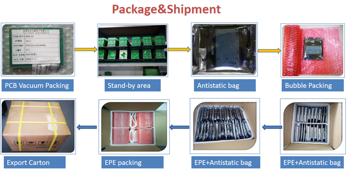
Strictly inspect before shipment and scan the code for verification to prevent unqualified products from being shipped.
FAQ:
1. What is your produce ability?
Our ability is average 30,000 square meters per month.
2. I only have the pcb sample, not pcb file, can you produce it for me?
Yes, we can copy file based on your sample, this file names gerber, and production then is accorded to gerber file.
3. What is your Lead time?
Lead time is usually punctual here, usually 5-10 days for PCB sample, 10-15 days for mass production. For some special situation, we can also advise customer in advance to avoid any non- expectation or loss at customer side.
4. What color is the solder mask and is there other colors available?
Our standard color for solder mask is green. We can also provide solder mask in red, blue or black for an additional amount.


