


ENIG stands for Electroless Nickel Immersion Gold. People also call it chemical nickel immersion gold. It is a surface finish used on printed circuit boards (PCBs). People often shorten it to ENIG or call it a chemical gold board. Today many PCBA boards inside mobile phones use ENIG. Some BGA carrier boards also use ENIG.
Compared with electroplated nickel-gold, ENIG does not need electricity on the board during the plating steps. It also does not need a wire to be pulled to each pad to plate nickel and gold. Because the process is simpler, producers can make many boards fast. The result is higher output and lower cost.
ENIG production flow
Here are two common production sequences. The first is the normal ENIG flow. The second is the thick-gold flow for pads that need more gold.
Typical ENIG flow:
Horizontal preclean → Load boards → Degrease (oil removal) → Rinse with water (x2) → Micro-etch → Rinse with water (x2) → Acid clean → Pure water rinse (x2) → Pre-dip → Activation → Pure water rinse (x3) → Chemical nickel deposit (Ni/P) → Pure water rinse (x2) → Immersion gold → Recovery → Pure water rinse (x2) → Unload → Board wash → Board inspection
Thick-gold flow:
Horizontal preclean → Load boards → Degrease → Rinse with water (x2) → Micro-etch → Rinse with water (x2) → Acid clean → Pure water rinse (x2) → Pre-dip → Activation → Pure water rinse (x3) → Chemical nickel deposit (Ni/P) → Pure water rinse (x2) → Pre-dip for gold → Thick gold deposit → Recovery → Pure water rinse (x2) → Unload → Board wash → Board inspection
Key step explanations — simple
Pre-treatment: The goal is to brush or sandblast the copper to remove oxide. This also roughens the copper surface. Roughing helps nickel and gold stick better later.
Micro-etch: Use sodium persulfate or sulfuric acid to remove the oxide on copper. Micro-etch also reduces deep scratches caused by brushing. Deep brush marks can help immersion gold attack the nickel later.
Activation: Copper cannot start the chemical nickel deposition by itself. So first we put a thin layer of palladium (Pd) on the copper. Palladium acts as a catalyst for the nickel deposition. The chemistry uses the fact that copper is more active than palladium. Palladium ions reduce to palladium metal and stick to the copper surface.
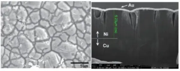
Chemical nickel (Ni/P): This is a nickel-phosphorus deposit. Its main job is to stop migration and diffusion between copper and gold. It also reacts with solder during soldering to form intermetallic compounds (IMC). In other words, the nickel layer keeps copper from moving into the solder and helps solder bond.
Immersion gold: Gold protects the nickel from oxidation. Gold does not react in the soldering chemistry. Too much gold can reduce solder joint strength. So the gold layer only needs to cover the nickel well enough to prevent oxidation. If you do Chip On Board (COB) wire bonding, you need a thicker gold layer. For most surface pads, a thin layer around 0.05 µm (2 µ”) or thinner is common. This thin layer is easy to control and lowers cost compared with electroplated nickel-gold.
Why ENIG gold is thin and the risk
Because ENIG gold is very thin, it only protects nickel from air and corrosion. If the gold is not enough, nickel will contact air and corrode. Or the gold can be over-etched by the acidic gold bath. Both cases can cause “black nickel” or “black pad”. The gold layer may still look shiny by eye. So visual check is not reliable. It is very important to check ENIG PCB quality before assembly.
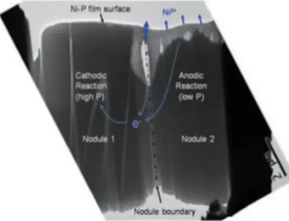
Black nickel — how it forms and why it is bad
Nickel layer quality depends on the nickel bath formula and temperature control during chemical deposition. The immersion gold step also affects the result. The chemical nickel process uses hypophosphite (sodium hypophosphite) and nickel salts in a self-catalyzed reaction. The deposit includes some phosphorus (P). Studies show that the normal phosphorus content in the nickel deposit should be about 7% to 10%. If the bath is not kept well or temperature control fails, phosphorus content will fall outside this range.
If phosphorus is too low, the nickel layer becomes easy to corrode. This corrosion often starts from the acidic gold bath attacking the nickel. If phosphorus is too high, the deposit becomes hard. That lowers solderability. It also hurts the formation of reliable solder joints.
If the nickel deposit has low phosphorus and the immersion gold step is not handled well, the gold layer may crack a lot. During later cleaning, the acidic gold bath can be hard to remove. Exposed nickel will corrode faster in air. This leads to black nickel, also called black pad. Black pad causes bad solder joints.
When black nickel forms, the gold layer on the board surface may still look shiny and gold. So people may think the pad is fine. During high temperature soldering, the gold layer dissolves quickly into the solder paste. The corroded nickel cannot react with molten solder to make intermetallic compound (IMC). This lowers the reliability of the solder joint. Joints then crack easily under small external forces.
Phosphorus-rich layer — formation and harm
In ENIG, the metal that alloys with solder is the nickel. The typical intermetallic compound (IMC) is Ni3Sn4. Phosphorus in the nickel does not join the metal compound. But phosphorus is present in the nickel deposit and it is spread evenly. When nickel reacts and forms IMC, leftover phosphorus gathers. It concentrates at the edge of the IMC and forms a phosphorus-rich layer.
If the phosphorus-rich layer is too thick, its strength is low. When a solder joint sees stress, the weakest spot breaks first. Often the phosphorus-rich layer is that weak spot. Then the solder joint reliability falls.
This is worse in high-heat lead-free processes. If process control is poor, IMC gets thick. More IMC means more leftover phosphorus. So the phosphorus-rich layer grows. The result is a higher risk of solder joint failure. The phosphorus-rich layer can be seen as a dark band between the IMC and the nickel. Energy dispersive X-ray spectroscopy (EDS) shows this band has very high phosphorus content. Many failure cases show the phosphorus-rich layer causes joint cracking.
How to prevent black nickel and phosphorus-rich layer
Both black nickel and phosphorus-rich layers are hidden defects. Normal visual checks can miss them. But if we know their causes, we can use good controls to prevent them.
For black nickel:
Maintain the nickel plating bath and keep temperature stable. This helps keep nickel-phosphorus ratio in the right range.
Maintain the acidic gold bath. If the gold bath is too corrosive, adjust it in time.
Control the pre-treatment well. Avoid deep brush lines. Remove residues well.
Control activation and rinses so palladium seeding is uniform and nickel deposits well.
Control immersion gold time so gold does not crack.
For users and buyers, check ENIG quality before assembly. There are several methods:
Use scanning electron microscope (SEM) to look at the pad surface. Check if the gold has cracks. Use EDS to measure phosphorus ratio in the nickel. This gives a clear micro view.
Manual solder test. Hand-solder typical pads, then measure pull or shear strength of the joint. If pull strength is much lower than normal, black nickel may exist. This test is easy and quick.
Acidic gas corrosion test. Expose ENIG samples to acidic gas. If powder forms or the surface discolors, it means the gold layer has cracks. That shows likely black nickel.
Out of these, the second method is most convenient and fast. It is simple to do. With these checks you can find problems before assembly. That reduces the number of boards that fail later and lowers loss.
Controlling the phosphorus-rich layer
To reduce the phosphorus-rich layer, keep the nickel-phosphorus ratio in the right range in the deposit. Also control the soldering process. Control solder time and solder temperature. Aim to keep the IMC thickness near the best range of about 1–2 microns (µm). If IMC becomes too thick, more phosphorus will concentrate. That makes the phosphorus-rich layer worse.
In short, good bath maintenance, temperature control, and precise soldering profiles are key. These steps keep IMC thin and the phosphorus-rich layer small. Then solder joint reliability stays high.
Summary — simple points
ENIG is electroless nickel followed by immersion gold. It is common in phone PCBA and some BGA carriers.
ENIG is cheaper and simpler than electroplated nickel-gold because it does not need electrical plating or pad wiring.
Main steps are pre-treatment, micro-etch, activation with palladium, chemical nickel (Ni/P), and immersion gold. There is also a thick-gold variant for special needs.
Chemical nickel blocks copper-gold migration and helps form solder IMC. Immersion gold protects nickel from oxidation. Gold is thin and only needs to protect nickel. Too much gold hurts solder strength. For wire bonding (COB) use thicker gold.
Black nickel (black pad) happens when nickel has wrong phosphorus content or when gold layer cracks. Black nickel can hide under shiny gold. It causes poor soldering and cracks.
Phosphorus-rich layers form near the IMC edge when nickel contains phosphorus. Thick IMC and poor process control make this worse. The phosphorus-rich layer lowers joint strength and causes cracking.
Prevent problems by keeping nickel bath and gold bath well maintained, controlling temperature, avoiding deep brush marks, and controlling solder profiles.
For quality checks use SEM/EDS, manual solder pull tests, or acid gas corrosion tests. Manual solder pull is the fastest and easiest.
Keep IMC thickness near 1–2 µm in lead-free processes to lower the risk of phosphorus-rich layer failure.