
ENIG PCB Manufacturing
A thin gold protective surface over a nickel barrier, applied to the exposed lands of your circuit board for solder assembly.
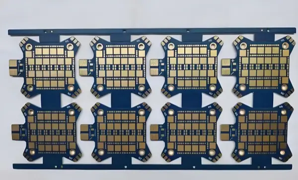
FLJ supplies ENIG-finished bare boards and coordinated PCB assembly, with nickel and gold requirements carried through fabrication and finish inspection.
ENIG-Finished Circuit Boards
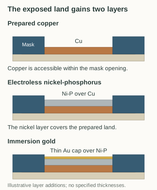
ENIG forms a solderable finish on the intended exposed copper features. It combines electroless nickel-phosphorus with a thin immersion-gold cap, giving each metal a distinct job at the pad.
Gold Protection and the Nickel Soldering Interface
The nickel-phosphorus deposit separates the copper conductor from the outer interface. The gold cap protects that surface during handling and storage before assembly.
During soldering, the thin gold layer normally dissolves into the molten solder. The nickel-bearing region then participates in the solder-joint interface while continuing to separate it from the copper. This is why an ENIG solder land and a gold contact designed for repeated mating have different surface requirements.
Fine-Pitch Pads and Board Topography
A thin, conformal finish supports consistent soldering lands for BGA, QFN and other fine-pitch layouts. It follows the underlying copper surface, so land geometry and the complete board construction remain important.
ENIG does not fill an open or recessed via or correct board warpage. Where a package needs a continuous flat land, the via construction and copper surface must provide that foundation before the finish is applied.

Nickel and Gold Thickness Specifications
The finish specification identifies nickel and gold separately, with a unit for each value. Where IPC-4552 is specified, the order identifies its revision together with the project-specific measurement, sampling and acceptance requirements.
Scroll to compare the two metal layers and their requirements →
| Metal layer | Role at the pad | Thickness requirement | Verification object |
|---|---|---|---|
| Electroless Ni-P | Barrier between copper and the outer interface; participates in the soldering interface | State the nickel-layer thickness in µm, including the required tolerance or limits | Nickel-layer result from the appropriate coating model |
| Immersion Au | Protective gold cap before soldering | State gold thickness in µm or µin, with the unit retained throughout the drawing and report | Gold-layer result, recorded separately from nickel |
Exact conversion: 1 µin = 0.0254 µm.
An illustrative nominal stack of 5 µm nickel and 2 µin gold contains 5 µm Ni-P (about 196.85 µin) and 0.0508 µm Au. Each value belongs to its own metal layer; the units remain attached to the requirement.
Nominal example for reading units; the released specification defines production thicknesses and acceptance.
How ENIG Is Manufactured
FLJ applies ENIG to the intended exposed copper features after the relevant solder-mask pattern has been formed. The manufacturing sequence prepares those surfaces, builds the nickel layer and adds its gold protection.
Copper Preparation and Electroless Nickel
Cleaning and micro-etching prepare the exposed copper, followed by the suitable activation sequence. Surface contamination or an inconsistent starting surface can affect the deposit that follows.
A controlled chemical reaction builds the nickel-phosphorus layer on the prepared features. The process controls the deposit through bath condition, loading, temperature and exposure, with the required layer thickness as a defined manufacturing target.
Immersion Gold, Rinsing and Drying
In conventional immersion-gold deposition, nickel at the exposed surface is oxidized and dissolves while gold ions are reduced to metallic gold. The protective cap forms through this exchange at the nickel interface. Excessive or uneven nickel attack can weaken that interface, so nickel condition, gold-bath condition and exposure are controlled together.
Rinsing and drying remove process residues and prepare the finished boards for inspection and protective packing. Surface preparation, deposition and final cleaning work together to produce the completed ENIG lands.
Control the surface being made. Bath chemistry and condition, process loading, time, temperature and carryover each affect the route from prepared copper to a finished nickel-gold interface.
Finished boards can proceed into SMT printing, placement and reflow as part of a coordinated assembly order. The ENIG finish and the soldering process serve the same land pattern at different stages of the build.
ENIG Inspection and Process Control
The finish is checked against its separate metal requirements and the condition needed for assembly. Layer thickness, the nickel interface and solderability each answer a different manufacturing question.
Metal-Specific XRF Measurement
X-ray fluorescence measures the coating system using a model suited to gold over nickel-phosphorus and copper. Calibration references, the instrument’s measurement capability and the feature being examined must suit that stack.
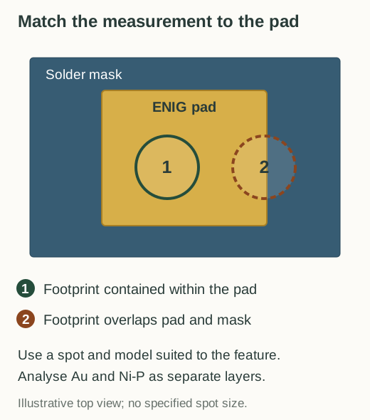
The measurement footprint belongs within the intended pad. Overlapping solder mask, a feature edge or another material can change what contributes to the result. Small functional lands and larger process coupons therefore need a deliberate measurement plan.
Nickel and gold results are recorded separately, with their units and measurement locations. A report should keep those layer-specific values connected to the relevant board or coupon.
Nickel Corrosion and Solderability
Black-pad concerns relate to excessive corrosion of the electroless nickel and a weakened interface. Control of the nickel deposit and the gold-deposition conditions addresses the surface where that damage can develop. Phosphorus is a normal part of the Ni-P deposit; its presence alone does not identify a defect.
Thickness measurement does not replace evaluation of nickel condition or soldering response. Targeted interface and solderability checks can be included in specialized PCB verification, with the method and sample locations matched to the question being investigated.
Assembly Interfaces, Handling and Finish Choices
Choose the finish around the work performed at the exposed surface. Soldering, repeated contact and bonding place different demands on the same gold-coloured area.
Solder Pads and Selective Hard-Gold Contacts
- Solder assembly
- ENIG provides nickel-gold finished lands for the intended paste printing and soldering route, including fine-pitch component layouts.
- Repeated mating contacts
- Wear-oriented contacts can use selective hard gold alongside ENIG soldering regions. The contact surface and the soldering pads retain their own finish requirements.
- Bonding interfaces
- Bond pads need a finish qualified for the selected wire material and bonding process. For mixed soldering and bonding, the available surface-finish routes include ENEPIG as a candidate for that specific bond process. A soldering finish is selected against different interface requirements.
- Exposed RF conductors
- The nickel-bearing surface is considered against the operating frequency, exposed trace or transition geometry, and loss budget. Where the finish makes a significant contribution, a nickel-free alternative can be evaluated within the RF board construction.
Protecting the Finish Before Assembly
Clean handling and protective packaging preserve the exposed lands between fabrication and soldering. Manufacturing lot, packing date and storage history help keep that surface connected to the assembly plan.
The usable storage interval depends on the finish process, packing and exposure conditions. Reflow, selective soldering, rework and extended holds also belong in the planned manufacturing route.
Keep pads protected from direct handling and contamination, and retain the specified packing and storage conditions until the boards enter assembly.
Specify Your ENIG PCB Build
Send the board files, nickel and gold requirements, quantity and inspection needs. The quotation reflects the exposed finish area, metal targets and manufacturing scope, with bare-board or coordinated assembly supply.