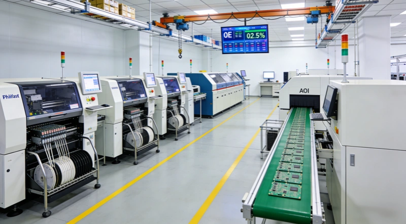

















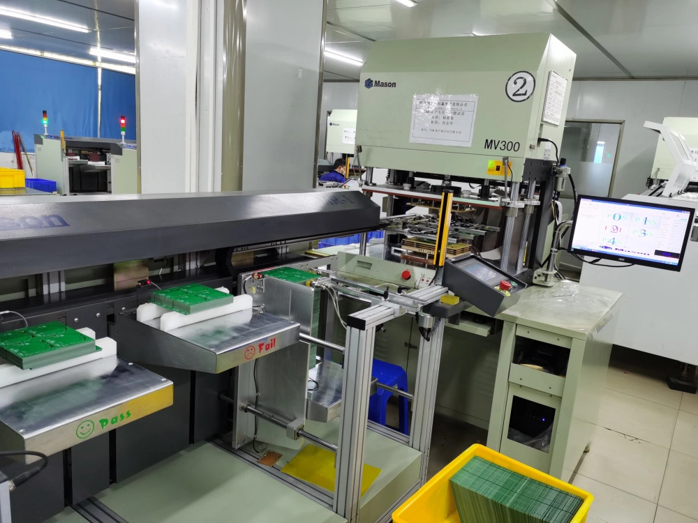
A multilayer PCB rarely fails because one production step was “bad.” More often, the layout, stack-up, drill strategy, and inspection plan were not aligned before fabrication began. Once internal layers are pressed into one panel, correcting an internal-layer mistake is no longer practical.
A standard rigid multilayer board is built by imaging and etching individual inner layers, bonding those layers with prepreg and copper foil under controlled heat and pressure, then drilling, plating, patterning, protecting, testing, and profiling the finished panel. The exact route changes with the construction—such as blind vias, buried vias, HDI microvias, controlled impedance, heavy copper, or specialty laminates—but this basic sequence remains the foundation.
Key takeaway: A manufacturable multilayer PCB depends on four decisions made early: a documented stack-up, realistic design rules, a drill/via strategy compatible with the fabricator, and inspection requirements that match the product’s risk.
What makes multilayer PCB fabrication different?
A PCB i flere lag contains three or more conductive copper layers separated by insulating dielectric materials. Internal signal, power, and ground planes allow designers to route more circuitry in a smaller footprint while managing return paths, impedance, power distribution, and electromagnetic coupling more effectively than a simple one- or two-layer construction can.
That capability also creates manufacturing dependencies: registration, resin flow and cure, hole-wall metallization, external circuitry, surface protection, dimensions, and electrical integrity all have to match the released design data.
View the process in two parts:
| Process stage | Primary purpose | Typical engineering question |
|---|---|---|
| Data preparation and inner-layer build | Turn released design data into accurate internal copper circuitry | Can the proposed trace, space, pad, annular ring, and stack-up be built repeatedly? |
| Lamination, interconnection, and finishing | Bond layers, create conductive holes, complete external features, and verify the board | Will the board remain electrically connected, solderable, dimensionally correct, and inspectable? |
1. Pre-production engineering: turn design data into a build plan
The manufacturing process starts with data, not with copper. A fabricator typically receives fabrication data such as Gerber, ODB++, or IPC-2581, together with drill files, drawings, netlist information, fabrication notes, and—when assembly is in scope—a BOM and assembly package. The production engineering team uses those inputs to create manufacturing instructions for imaging, drilling, routing, inspection, and process control.
This is where a design for manufacturability (DFM) review provides the greatest leverage. The review should clarify layer count, finished board thickness, copper weights, controlled-impedance requirements, material family, surface finish, minimum trace and space, minimum finished hole size, via types, solder mask treatment, rout profile, panelization, and applicable acceptance criteria. A missing note does not always stop fabrication, but it can force a supplier assumption that conflicts with the design intent.
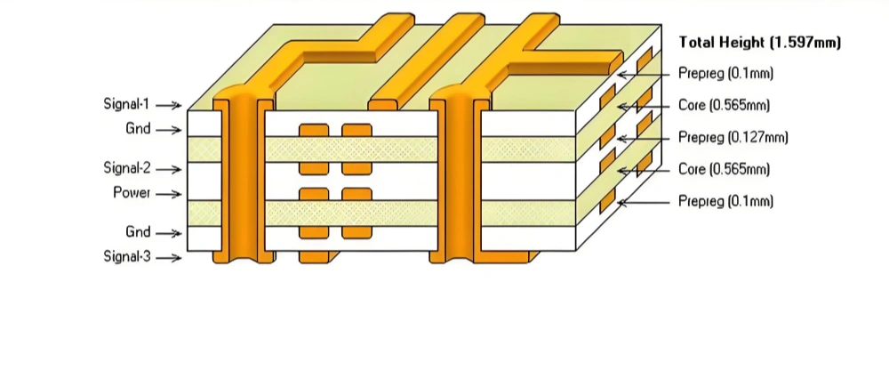
For multilayer boards, the stack-up is especially important. A stack-up is not merely a diagram showing copper layer order. It defines the dielectric separations and material construction that influence impedance, plane capacitance, thermal behavior, stiffness, layer registration strategy, and final thickness. Prepreg is uncured resin-impregnated glass fabric; during lamination its resin flows, fills appropriate spaces, and cures to bond the construction.
What to resolve before release
Before sending files for quotation or fabrication, confirm the following items with the intended manufacturer:
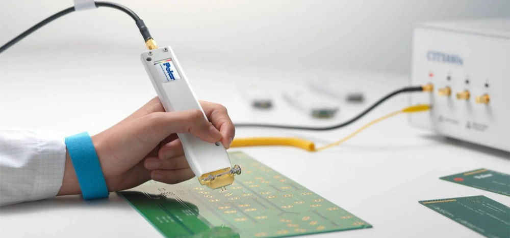
- Which layers carry controlled-impedance traces, and what target impedance and tolerance are required?
- Are there blind, buried, back-drilled, filled, capped, or laser-drilled vias that require a different build sequence?
- Which copper layers are planes, and does the copper balance create a risk of uneven resin flow or warpage?
- Does the fabrication drawing define finished dimensions, hole tolerances, edge features, countersinks, and controlled-depth features?
- Are the test requirements clear: netlist electrical test, impedance verification, microsection, solderability, or other customer-specific checks?
2. Inner-layer imaging and etching: create the circuits that will be sealed inside
For a conventional multilayer rigid board, fabrication begins by preparing copper-clad core material for the internal layers. A photosensitive resist is applied, the circuit artwork is transferred using UV imaging or laser direct imaging, and the panel is developed so unwanted copper can be removed by etching. The remaining resist is stripped, leaving the intended copper circuitry.
The process may sound straightforward, but inner layers carry a unique risk: they will later be inaccessible. A short, open, trace-width loss, registration error, or etch defect discovered after lamination can become a scrapped panel rather than a reworkable issue. That is why inner-layer automated optical inspection (AOI) is commonly used before the layers enter the press cycle. AOI compares the physical pattern with a digital reference to find feature discrepancies that warrant review.
Designers can make this stage easier by avoiding unnecessary extremes. Very fine trace/space geometries, large copper-density differences, isolated copper islands, and ambiguous polarity or layer naming all increase the chance of engineering queries or process adjustments. If a tight feature is essential, specify the electrical and functional reason rather than assuming that a nominal CAD dimension alone communicates the real requirement.
3. Surface preparation and lamination: convert separate layers into one structure
After the inner layers have been inspected, their copper surfaces are prepared to support adhesion. The layers are then arranged in the specified order with prepreg between appropriate layers and copper foil on the outer surfaces. Controlled heat, pressure, and time allow resin to flow and cure so that the stack becomes one solid multilayer panel.
Lamination is a manufacturing checkpoint, not a passive bonding step. The construction must balance several competing needs: enough resin flow to fill copper topography and bond the layers, but not so much uncontrolled flow that it disturbs intended dielectric thickness or creates defects. The fabricator’s press cycle, material system, copper distribution, and construction all affect the result.
The practical lesson is that designers should not treat every FR-4 stack-up as interchangeable. For a high-speed or RF-sensitive design, the approved laminate family, copper roughness assumptions, dielectric thicknesses, and final impedance model should be aligned with the actual fabricator’s material availability and press construction. For a high-current design, copper weight, plane distribution, thermal paths, and drilling implications may matter more than signal loss alone.
4. Registration, drilling, and hole-wall preparation
Once laminated, the panel needs holes for plated-through interconnections, component leads, tooling, or mechanical features. Registration systems use internal targets to align the drilling operation with the buried copper features. Mechanical drilling is common for many through holes; laser drilling is associated with certain fine-pitch and high-density interconnect constructions.
Drilling creates a second manufacturing challenge: the newly exposed hole wall contains dielectric material as well as copper targets. Heat and mechanical action can leave resin smear or debris that interferes with the conductive path needed later. A desmear or related hole-preparation process is therefore used to clean and prepare the drilled holes before metallization.
At this stage, the drill and via plan deserves careful DFM attention. Small holes, deep aspect ratios, tight annular rings, multiple sequential build-ups, and complex back-drill requirements can all change capability, yield, and cost. A robust design starts by asking not only, “Can this via connect the nets?” but also, “Can this via be drilled, cleaned, plated, inspected, and repeated at production volume?”

5. Electroless copper and electroplating: make the vertical interconnects conductive
The hole walls are initially nonconductive in the dielectric sections. To establish a conductive base, fabricators use electroless copper deposition after hole preparation. Electrolytic copper plating then builds copper on the panel surface and in the hole walls, enabling reliable interlayer connections and the required conductor thickness.
A via cannot be evaluated solely by its CAD diameter. Its reliability depends on the complete system: drill quality, hole-wall preparation, plating control, copper distribution, stack-up behavior, thermal exposure, and annular-ring allowance.
A clear fabrication package should distinguish finished hole size from drill size where necessary, identify plated and non-plated holes, and define special via treatments. If the assembly depends on via-in-pad, filled and capped vias, or plugged vias, say so explicitly; those constructions require additional process choices.
6. Outer-layer imaging, pattern plating, and final etching
Outer-layer processing creates the final surface circuitry. Photoresist is applied and imaged to define where copper will remain or be built. Copper and protective tin can be plated in the required locations; remaining resist is stripped; unwanted copper is etched; and the temporary tin protection is removed. The core objective is to leave the specified external traces, pads, and plated features while maintaining registration to the internal layers and drilled holes.
Because the outer layers interact directly with components and connectors, this step has clear assembly consequences. Pad geometry, solder mask clearance, copper balance, fine-pitch features, edge-plating requirements, and connector contact zones should be reviewed in the context of the intended assembly process.
7. Solder mask, legend, and surface finish: protect copper and prepare for assembly
A solder mask is applied and patterned so that solderable areas remain exposed while other copper features receive environmental and electrical protection. Legend marks are then used for component references, polarity, revision information, traceability, or other board identification.
The exposed pads require a surface finish to protect copper from oxidation and support soldering. Common finish families include HASL, lead-free HASL, ENIG, immersion silver, immersion tin, and OSP, although the appropriate choice depends on the assembly process, storage needs, component pitch, contact wear, environment, compliance requirements, and cost model.
| Selection issue | Why it matters | What to define in the manufacturing package |
|---|---|---|
| Overfladefinish | Affects solderability, flatness, shelf-life behavior, and compatibility with contacts or wire bonding | Finish type, applicable standards, special contact areas, and any assembly constraints |
| Solder mask treatment | Influences insulation, pad definition, via treatment, and assembly behavior | Mask color if required, mask-defined or non-mask-defined pads, via tenting/plugging/filling requirements |
| Legend | Supports assembly, test, servicing, and traceability | Reference designators, polarity markings, revision marks, restrictions around pads and fine features |
8. Electrical test, final inspection, profiling, and packaging
Before shipment, a bare-board electrical test can check continuity and isolation against the intended netlist, helping identify opens and shorts. Final inspection also addresses workmanship, dimensions, surface condition, and other acceptance requirements. A supplier’s exact sampling plan, acceptance criteria, and test coverage should be agreed in the purchase specification rather than assumed from a generic statement such as “100% tested.”
The panel is then profiled into individual boards or deliverable arrays using methods such as routing or V-scoring, depending on the product’s separation, edge-quality, stiffness, and assembly needs. Packaging is not an afterthought: boards should reach assembly clean, dry, traceable, and protected in a way that supports the chosen finish and expected storage conditions.
The most common process risks—and how to prevent them
Multilayer fabrication risk is usually manageable when the right question is asked early. The following patterns frequently generate avoidable delays, cost increases, or yield concerns.
| Risk pattern | Root cause | Better engineering response |
|---|---|---|
| Impedance misses | The stack-up used for simulation does not match the approved production material and dielectric construction | Obtain the fabricator’s proposed stack-up and validate critical controlled-impedance structures before release |
| Inner-layer scrap | Fine features, polarity mistakes, or artwork ambiguities are found after imaging or lamination | Run DRC, provide clear layer naming, and resolve design-rule exceptions during pre-production review |
| Via reliability concern | Hole geometry, plating demand, material behavior, and thermal stresses were considered separately | Review the complete via strategy with the fabricator, including finished holes, annular rings, aspect ratio, fill/cap needs, and application environment |
| Lamination or warpage concern | Copper distribution, resin needs, and stack symmetry were not evaluated together | Use a balanced, intentional stack-up and discuss unusual copper patterns, cavities, or thickness transitions early |
| Assembly defects blamed on fabrication | Finish, mask, pad, stencil, component, and profile requirements were not coordinated | Review fabrication and assembly packages together; identify fine-pitch, thermal-pad, BGA, connector, and test-access constraints |
What should you send for an accurate multilayer PCB review?
For a useful technical review, provide released fabrication data, drill data, a fabrication drawing, stack-up or impedance notes, material requirements, target quantity, delivery objective, and a netlist where available. For assembly, add the BOM, centroid or pick-and-place file, assembly drawing, special-process requirements, and test strategy.
Flag anything that cannot change, such as connector locations, impedance targets, controlled-depth features, critical dielectric thicknesses, contact finish, or mandated acceptance requirements.
Frequently asked questions
How many layers does a multilayer PCB have?
A multilayer PCB has three or more conductive copper layers separated by dielectric material. In practical design and manufacturing discussions, the most useful question is not simply the layer count but how the layers are assigned to signals, power, ground, controlled-impedance structures, and routing escape.
What is the most critical step in the multilayer PCB manufacturing process?
There is no single universal answer. Data preparation, stack-up definition, inner-layer accuracy, lamination control, drilling/plating quality, and electrical verification are interdependent. For many projects, the earliest DFM and stack-up review provides the greatest opportunity to prevent later production issues.
Why is lamination so important in a multilayer board?
Lamination bonds the inner layers, prepreg, and outer copper into a solid structure. The resin flow, cure condition, pressure, temperature, and construction affect adhesion, dielectric structure, and the board’s overall integrity.
Are plated-through holes and microvias made the same way?
Not necessarily. Conventional plated-through holes are commonly mechanically drilled through the laminated construction, while laser drilling is often used for specific high-density interconnect structures. The required build sequence depends on the intended via type and stack-up.
Should I choose a surface finish before sending the board for fabrication?
Yes. Surface finish is tied to solderability, component pitch, storage, assembly method, contacts, compliance requirements, and budget. It should be included in the released fabrication notes, not selected as an afterthought.
Final thought
The best multilayer PCB manufacturing process is not simply the fastest sequence of factory steps. It is a controlled translation of your design intent into a stack-up, fabrication route, and verification plan that a supplier can build repeatedly. Send your Gerber or IPC-2581 data, stack-up requirements, drill notes, and assembly constraints for a DFM-focused engineering review before production release.