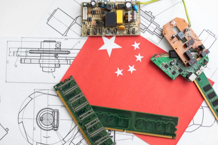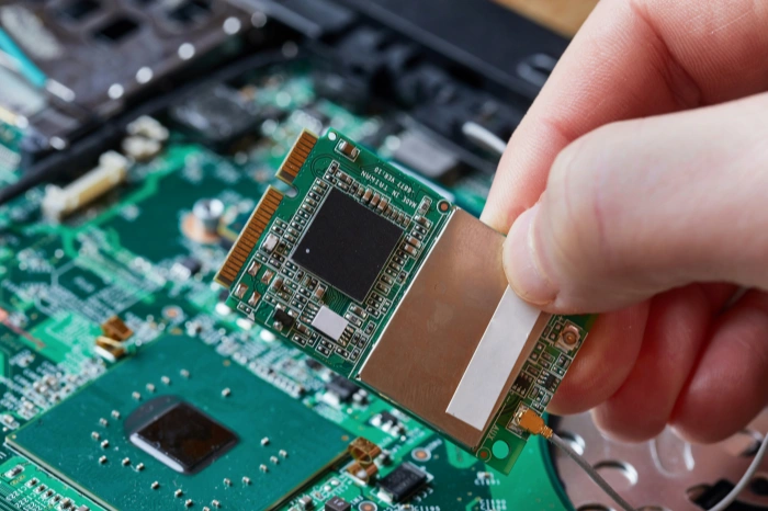
If you’ve ever used a digital clock, calculator, TV remote, router, laptop, or even a kid’s toy, you’ve used a PCB. Multiple PCBs, usually.
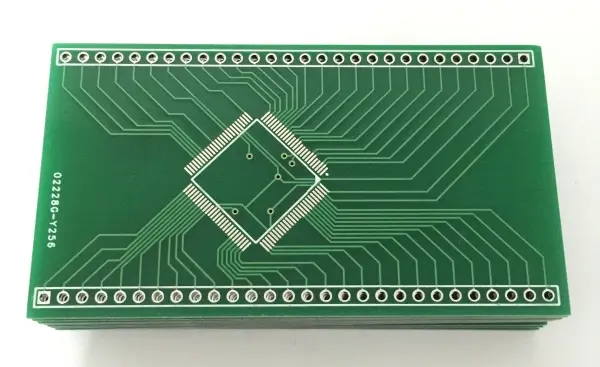
At the simplest level, a PCB board is an insulated board with conductive copper pathways that connect electronic components together. Those copper routes direct current and signals where they need to go, and the board also holds everything in place mechanically so the circuit is not just a fragile mess of loose wires.
And yes people say “PCB board” all the time even though it’s a bit redundant (the B already means board). Still, it’s common, so we’ll roll with it.
A PCB in plain English
Think of a PCB like a city map for electricity.
- Die components (chips, resistors, capacitors, connectors) are the buildings.
- Die copper traces are the roads.
- Die pads are the parking lots where parts get soldered.
- Die Durchkontaktierungen are elevators that move signals from one floor to another (one layer to another).
Every copper route matters. The width, spacing, length, where it runs, what it runs next to. That “path” determines how the circuit behaves, especially for high-speed or high-frequency designs.
So a PCB board isn’t just “a thing you mount parts on”. It’s part of the circuit.
What does PCB stand for (and what is PWB)?
PCB = Printed Circuit Board.
You might also hear:
- PWB = Printed Wiring Board.
- Some people use it to mean the bare board (the substrate and copper patterns) before components are assembled. In everyday conversation, PCB and PWB get mixed a lot.
And then there’s PCBA = Printed Circuit Board Assembly, which is the PCB after components are placed and soldered.
Also, quick clarification because it comes up constantly.
A motherboard is a PCB, but not every PCB is a motherboard. A motherboard is just a big complex PCB that acts as the main hub in a computer.
What is a PCB made of?
Most common PCBs are built from:
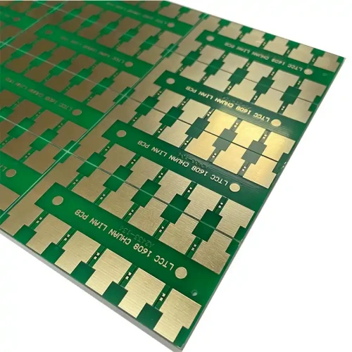
- Base material (substrate): usually FR4 (woven glass fiber + epoxy resin). Strong, stable, inexpensive.
- Copper: thin copper foil bonded to the substrate, then etched into traces.
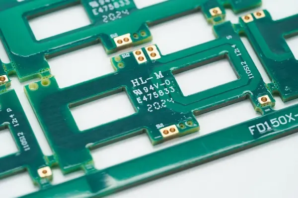
- Solder mask: that colored protective layer (often green). It helps prevent solder bridges and protects copper from corrosion.
- Silkscreen: the white (or black) printed text and markings. Component labels, logos, pin 1 markers, warnings, etc.
- Oberflächenbehandlung: a coating on exposed pads to make soldering reliable and prevent oxidation. Options include HASL, ENIG (gold), immersion silver, and more.
So when you look at a PCB, you’re really seeing a stack of materials designed to satisfy both electrical needs (signal routing, impedance, grounding) and mechanical needs (mounting, durability, stability).
Why PCBs matter so much (more than people realize)
PCBs are important because they do a bunch of jobs at once:
- Circuit interconnection: clean, repeatable connections between parts.
- Structural support: they hold components firmly in a compact shape.
- Circuit protection: solder mask and layout spacing reduce shorts and contamination issues.
- Production efficiency: assembly lines can place and solder parts fast (especially SMT).
- Maintenance and upgrading: easier to test, repair, or revise compared to hand wiring.
- High-density integration: modern electronics would be basically impossible without multilayer boards, fine traces, and small vias.
And reliability matters. A defective PCB inside a finished product can be brutally expensive to fix once it’s out in the world. That’s why DFM and testing are a big deal.
Common PCB types (the ones you actually see in the wild)
There are a lot of ways to classify PCBs, but these are the big ones.
1) Single-sided PCB
Copper on one side only. Simple, cheap, still used in basic electronics.
2) Double-sided PCB
Copper on both sides, connected with vias. More routing space, still fairly affordable.
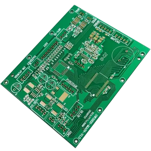
3) Multilayer PCB
Three or more copper layers. Modern devices often use 4-layer, 6-layer, 8-layer and up. A typical 4-layer stack might include:
- Top signal
- Inner ground plane
- Inner power plane (or signal)
- Bottom signal
Multilayer boards make routing cleaner, reduce noise, and support high-speed layouts. They also raise fabrication complexity.
4) Rigid, flex, and rigid-flex
- Rigid PCB: the standard solid board.
- Flex PCB: thin flexible circuits used in phones, cameras, wearables, tight spaces.
- Rigid-flex PCB: combination of both. More expensive but solves packaging problems.
5) High-frequency / high-speed PCBs
Used for RF, wireless, fast digital interfaces, and anything impedance-sensitive. These often need special materials with low dielectric loss, such as PTFE based laminates (and others like polyurethane, polyethylene, polystyrene mixes depending on the exact application and manufacturer offerings).

6) Special boards (a few you’ll hear about)
- Metal core PCB: used for heat dissipation and stability (common in LED lighting and power electronics).
- Surface mount PCB: not a “board type” exactly, more like an assembly style, but people say it. SMT supports light, thin, high-volume, lower-cost builds.
- Carbon film printed board: used where cost and simple process matter.
7) HDI PCB
HDI stands for high density interconnect. Smaller vias, tighter spacing, more wiring density than conventional PCBs. Used in phones, compact devices, advanced products.
How a PCB is designed (high level, but real)
PCB design is not just drawing lines until it “connects”.
A typical flow looks like this:
- Create the schematic diagram
- This is the logical circuit. What connects to what, values, nets, power rails. The “brain plan”.
- Create the blank PCB layout
- Define the board shape, mounting holes, keepout zones, connector positions.
- Capture and link schematic to PCB
- You import components (footprints) and connect nets so the PCB knows what must be connected.
- PCB stack-up design
- For modern designs, 4-layer FR4 is very common. The stack-up affects impedance, EMI, and manufacturability.
- Define design rules and DFM requirements
- Trace width, spacing, drill sizes, annular ring, solder mask clearance, impedance targets. These rules should match what the manufacturer can actually build. This is where designers often talk to fabricators and get their constraints.
- Platzierung der Komponenten
- Can be automatic for a start, but real placement is usually manual: signal integrity, heat, accessibility, assembly constraints. Placement is half the battle, honestly.
- Routing (wiring)
- Traces are laid out following guidelines. For high-speed designs, the solver or design tools can help control trace geometry for target impedance.
- Add identifiers
- Reference designators, polarity marks, test points, labels, logos. Small stuff that saves hours in assembly and troubleshooting.
- Run DRC checks
- Design rule check (DRC) catches spacing errors, missing connections, weird violations.
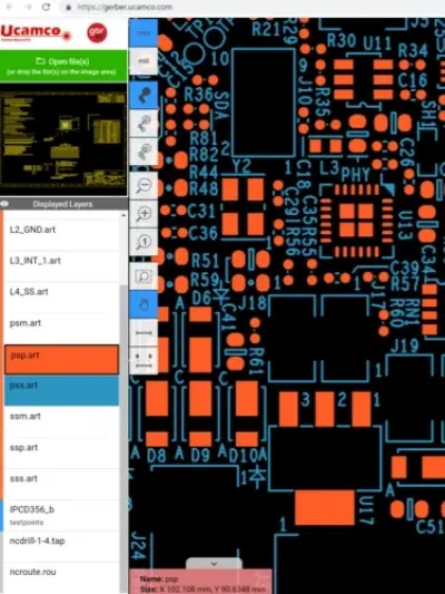
- Generate manufacturing files
- Usually Gerber (often extended Gerber) plus drill files, stack-up notes, and fabrication drawings.
Common PCB design software includes Altium Designer, OrCAD, Pads, KiCad, and Eagle.
How a PCB board is manufactured (the real step-by-step idea)
If you’ve never toured a PC board shop, it’s kind of addictive. Loud machines, chemical lines, stacks of panels, inspection stations. Designers who visit manufacturers usually come back more humble, because you start designing with manufacturing in mind after that.
Here’s a typical PCB manufacturing process, simplified but still accurate.
Step 1: Design and output
The PCB layout is created in CAD software and exported after checks, usually as Gerber files (often extended Gerber). This is the “source of truth” for fabrication.
Step 2: From file to film
A plotter prints photo films of the PCB design. The films are used to transfer the pattern onto the copper.
Step 3: Printing the inner layers
For multilayer boards, the inner layer copper pattern is created on copper foil that’s laminated to the substrate (epoxy resin + glass fiber). Photoresist is applied, exposed, and developed so the correct copper pattern can be formed.
Step 4: Removing the unwanted copper
Chemical processes remove excess copper while the hardened resist protects the copper that should remain. After etching, resist is stripped with solvent, leaving clean copper features.
Step 5: Layer alignment and optical inspection
Layers have to line up perfectly. Alignment punches and registration holes are used, and optical punch machines help position layers precisely.
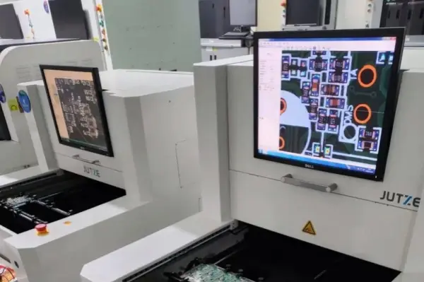
Then panels often go through automatic optical inspection (AOI). A laser sensor compares the panel to the Gerber data to spot opens, shorts, or pattern defects.
Step 6: Layer-up and bonding
The board is built like a sandwich. Layers of copper foil, prepreg (the bonding resin), and core material are stacked, often with press plates and aluminum foil, then pressed in a computer-controlled bonding press.
This is when the multilayer PCB becomes one solid unit.
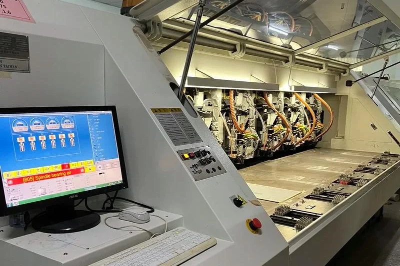
Step 7: Drilling
Holes are drilled for component leads, mounting, and vias. X-ray locators may be used to identify targets. CNC drilling machines can run extremely fast, with air-driven spindles up to around 150,000 rpm.
After drilling, extra copper or rough edges may be cleaned up with profiling tools.
Step 8: Plating (chemical deposition)
A thin layer of copper is deposited over the panel surface and inside drilled holes, so vias can conduct electricity between layers.
Step 9: Outer layer imaging
A new photoresist is applied to the panel. UV exposure hardens the resist where copper should remain. Unhardened resist is removed by machine.
Step 10: Outer layer plating (electroplating)
The board is electroplated with copper to build up thickness on traces and in vias, then often plated with tin to protect copper during etching.
Step 11: Final etching
Chemical solutions remove the excess copper. Tin protects the desired copper features. After etching, tin is stripped away as needed.
Step 12: Solder mask application
Epoxy solder mask ink is applied to both sides, then UV cured. Many boards also go through an oven cure for full hardness.
Step 13: Surface finish
Pads need a finish so they solder well and don’t oxidize. Options include:
- Chemical plating with gold (like ENIG) or silver
- Hot air leveling (HASL) to make pads uniform
There are multiple surface finish choices depending on cost, shelf life, and assembly method.
Step 14: Silkscreen
Ink-jet or screen printing adds vital information: reference designators, component outlines, polarity, logos, warnings.
Step 15: Electrical test
Boards are tested for opens and shorts. One common method is Flying Probe Testing, which checks electrical performance without needing a custom test fixture.
Step 16: Profiling and V-scoring
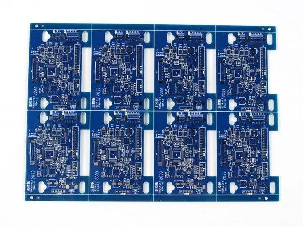
The final board outline is cut using a router, or V-grooves are added so boards can be snapped apart cleanly for panelized manufacturing.
Then packaging happens, often vacuum packaging for protection, then shipping.
That’s the core idea. Some factories add extra steps depending on the technology (HDI, blind/buried vias, controlled impedance coupons, etc.).
PCBs and modern wireless, high-frequency stuff
Electronics today is a lot of “signals behaving like radio” even when you don’t think it is. Fast digital edges, wireless transmission, voice, video, data. Everything has standards, and the PCB is where many of those performance battles are won or lost.
New generation products often push into:
- higher frequency boards
- low dielectric loss substrates
- tighter tolerances
- impedance controlled routing
If you’re doing RF, high-speed interfaces, or dense layouts, you usually can’t treat the PCB as an afterthought. It becomes part of the system.
So what is a PCB board, really?
It’s a manufactured platform that does two jobs at once:
- Routes electrical signals and power through copper pathways.
- Supports and protects the circuit mechanically so it can be assembled, shipped, used, and mass produced reliably.
That’s it. But it’s also why PCBs quietly run the world.
Need a reliable PCB board made?
Need a reliable PCB board for your next project? At Philifast, we provide high-quality PCB manufacturing with stable performance, fast turnaround, and professional support. Whether you need prototype boards or mass production, our team is ready to help you bring your design to life. Visit Philifast to get a quote today.
FAQs (häufig gestellte Fragen)
What is a PCB board and why is it important in electronics?
A PCB board, or Printed Circuit Board, is an insulated board with conductive copper pathways that connect electronic components together. It serves as the backbone of modern electronics by directing current and signals where needed, while mechanically holding components in place to prevent fragile wiring messes. PCBs are essential because they provide circuit interconnection, structural support, protection against shorts and contamination, production efficiency, ease of maintenance, and enable high-density integration in devices.
What does PCB stand for and how is it different from PWB and PCBA?
PCB stands for Printed Circuit Board. PWB means Printed Wiring Board and often refers to the bare board before components are assembled. PCBA stands for Printed Circuit Board Assembly, which is the PCB after components have been placed and soldered. While these terms are sometimes used interchangeably in everyday conversation, they highlight different stages or aspects of circuit boards.
What materials are commonly used to make a PCB?
Most common PCBs are made from several layers including: a base material (substrate) usually FR4 which is woven glass fiber combined with epoxy resin; thin copper foil bonded to the substrate that is etched into traces; a solder mask layer (often green) that protects copper from corrosion and prevents solder bridges; silkscreen printing for component labels and markings; and a surface finish like HASL or ENIG to ensure reliable soldering and prevent oxidation.
How do the copper traces, pads, and vias function on a PCB?
Copper traces on a PCB act like roads directing electrical current and signals between components (the buildings). Pads serve as parking lots where parts get soldered onto the board securely. Vias function as elevators moving signals between different layers (floors) of a multilayer PCB. The careful design of these pathways—including width, spacing, and routing—directly affects circuit performance especially in high-speed or high-frequency designs.
What are the common types of PCBs used in electronic devices?
Common PCB types include: single-sided PCBs with copper on one side used in simple electronics; double-sided PCBs with copper on both sides connected by vias offering more routing space; multilayer PCBs with three or more layers enabling cleaner routing and reduced noise for modern devices; rigid PCBs which are solid boards; flex PCBs which are thin and flexible for tight spaces like phones; rigid-flex PCBs combining both rigid and flexible sections; and high-frequency/high-speed PCBs designed with special materials to handle RF, wireless, or fast digital signals.
Why do modern electronics often use multilayer PCBs instead of single or double-sided ones?
Modern electronics use multilayer PCBs because they provide additional layers for signal routing, power distribution, and grounding which results in cleaner layouts with reduced electrical noise. Multilayer boards support high-speed layouts necessary for advanced devices by enabling fine traces and small vias. Although they increase fabrication complexity and cost compared to single or double-sided boards, multilayer PCBs are essential for high-density integration and reliable performance in complex electronic systems.