


Over time many electronic PCBs are no longer produced or updated, yet we may still need to repair and reuse these circuit boards in our equipment. When original design files are unavailable and components become obsolete, repair or improvement can be halted and entire devices may be discarded. PCB cloning and reverse engineering extend the life of electronic products. Especially when original PCB design data is lost, the manufacturer stops production, or some components are discontinued, engineers can perform PCB reverse analysis on the original board to reproduce circuit principles, rebuild schematics, and manufacture identical boards to ensure normal maintenance and operation. PCB reverse engineering is not only for copying but also for understanding fundamental design principles; when defects are found, engineers can re-route, modify designs, and optimize or upgrade products to meet more user requirements.
What is PCB Cloning?
PCB cloning is a reverse-engineering technique (also called PCB reverse engineering). When original design files (schematics, PCB source files) are missing, engineers disassemble the existing board and reconstruct it so that appearance and function match the original PCB. The process typically involves removing all electronic components from the original PCB, analyzing and testing each component to determine parameters and models, producing a clear BOM, scanning each PCB layer with precise imaging equipment, converting images to PCB design files with conversion software, and then producing and assembling new PCBs using the reconstructed files and BOM.
Why Clone a PCB?
Reasons for cloning include device repair, lowering development cost, and technical research/learning.
Technical and Engineering Reasons
- Fault analysis: Cloning helps locate hidden faults (intermittent failures, EMI, thermal failures) by restoring the circuit diagram to find root causes.
- Interface adaptation and compatibility: Cloning helps understand and implement adaptations to connect legacy devices to modern interfaces/protocols (e.g., network or communication modules).
- Aging and reliability improvements: Cloning can reveal weak components or layout defects for improvement.
Commercial and Cost Reasons
- Repair and maintenance: For expensive equipment, when the control PCB is damaged and the original board or components are unobtainable, cloning can restore the device at minimal cost and ensure long-term use.
- Supply-chain and cost optimization: When components are discontinued or costly, cloning allows substitution and cost reduction while ensuring stable part supply.
Research and Education
- Through reverse analysis, engineers learn layout, routing, power and signal-handling techniques from other experienced designers, improving R&D skills.
- Secondary development and feature improvements: Engineers can upgrade and customize functions based on the original design.
Step-by-Step: How to Clone a PCB
1. Create the BOM
In PCB cloning, the BOM lists every component’s parameters and specifications; it must clearly indicate component names, specs, models, and position IDs. From procurement to soldering and debugging, BOM accuracy is key to success.
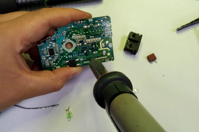
- Remove every component from the PCB. First take clear photos of the PCB to record component positions and orientations.
- Label each removed component with a position ID and attach it to paper for tracking; verify the numbering carefully.
- Component testing: test all removed parts and record parameters (use LCR meter, multimeter, curve tracer as needed) to measure resistors, capacitors, inductors, etc.
- Compile and verify the BOM against physical parts and test data (model, parameters, specs, brand).
- Procurement: purchasing relies on the BOM; incomplete or incorrect BOM data will prevent the cloned board from operating like the original.
2. PCB Copper-Layer Scanning
- Clean the bare PCB with alcohol, then place it on a scanner. Increase scan resolution, use Photoshop in color mode to scan silkscreen and save/print the file.
- Lightly sand the top and bottom copper layers with fine abrasive until copper shines; scan both layers in color mode. Adjust contrast/brightness so copper and non-copper differ clearly, convert to black-and-white, check trace clarity, and repeat if needed. Save final images as black BMP files (TOP.BMP and BOT.BMP). Use Photoshop for further corrections if necessary.
- Convert BMP TOP/BOT files to Protel/Altium format and import into Protel. If pads and vias align across layers, the scan is successful; otherwise repeat scanning.
3. Protel/Altium Synthesis
Synthesis work converts image files into Protel/Altium drawings.
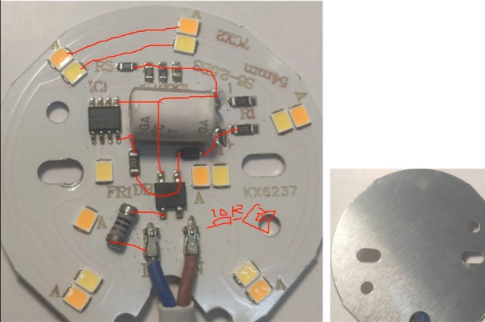
- Reconstruct schematics: In Protel Schematic, build power, clock, interface, and core circuits module by module; use library parts where appropriate and keep pin mappings and parameters consistent.
- Footprint mapping and placement: In the PCB library assign or create footprints that match actual pad sizes. Place components in the PCB document per the reference images to restore original layout and orientation.
- Trace routing: Route nets according to reference images; prioritize important signals (power, clocks, differential pairs) and preserve routing topology and density. For multilayer boards, use photos or X-ray to identify internal connections and rebuild copper layers.
- Verification and adjustment: Run ERC/DRC, netlist comparisons, and manufacturability checks; correct issues. Verify critical net connectivity on prototype boards with an oscilloscope or multimeter to ensure accurate reconstruction.
- Output and validation: Generate Gerber, BOM, and pick-and-place files; produce prototypes and perform functional and reliability tests.
With years of PCB industry experience, a complete reverse-engineering workflow, and professional testing/certification capabilities, PHILIFAST can provide efficient, compliant, and reliable PCB cloning services. From visual inspection, schematic reconstruction, and component replacement to prototype fabrication, functional verification, and long-term reliability testing, we apply rigorous technical standards and quality management to ensure every reproduced board meets or exceeds the original in performance, compatibility, and safety. Whether for spare parts, product longevity, or reengineering toward volume production, PHILIFAST is your trusted technical partner to reduce cost, secure supply, and accelerate project delivery.