1. Definition und Zeitpunkt des Hinzufügens von Ebenen
Für Hochgeschwindigkeits-Multilayer-Platten, Ein einfaches zweilagiges Design kann die Anforderungen an Signalqualität und Routingdichte oft nicht erfüllen. In diesem Fall müssen Sie dem Leiterplattenstapel weitere Lagen hinzufügen, um die Designanforderungen zu erfüllen.
2. Positive (Signal-)Ebenen und negative (invertierte) Ebenen
Eine positive Ebene ist die übliche Signalschicht, die für das Routing verwendet wird. Die sichtbaren Teile sind Leiterbahnen aus Kupfer. Auf einer positiven Ebene können Sie große Kupfermengen ausgießen und Bereiche mit Kupfer füllen, indem Sie z. B. Begriffe wie “Leiterbahn” oder “Kupfer” verwenden, um die Kupferbereiche zu beschreiben. Siehe Abbildung 8-32.

Eine negative Ebene ist das Gegenteil. Bei einer negativen Ebene wird in der Regel Kupfer über die gesamte Ebene gegossen. Die Routingbereiche sind die Ausschnitte. Auf den Routing-Linien befindet sich kein Kupfer. Sie müssen das Kupfer ausschneiden und dann die Netze für die ausgeschnittenen Bereiche setzen. Siehe Abbildung 8-33.

3. Aufteilung der inneren Strom-/Masse-Ebenen
In älteren Protel-Versionen wurden die inneren Leistungsebenen mit einer “Split”-Funktion geteilt. In aktuellen Versionen wie Altium Designer 19, Sie teilen, indem Sie “Linien” zeichnen und diese mit dem Hotkey “PL” platzieren. Die Trennlinien sollten nicht zu dünn sein. Sie können 15 mil oder mehr wählen. Wenn Sie nach dem Aufteilen Kupfer gießen, zeichnen Sie ein geschlossenes Polygon mit dem “Linien”-Werkzeug, doppelklicken Sie dann in das Polygon und legen Sie das Netz für den Kupferguss fest. Siehe Abbildung 8-34.

Sowohl positive als auch negative Ebenen können für innere Stromversorgungs- oder Masselagen verwendet werden. Sie können eine positive innere Ebene auch durch Routing und Kupfergießen erreichen. Der Vorteil einer negativen Ebene besteht darin, dass Sie standardmäßig mit einer großen gegossenen Kupferfläche beginnen. Dann können Sie Durchkontaktierungen hinzufügen oder die Gussgröße ändern, ohne die gesamte Lage neu zu gießen. Dies spart Zeit bei der Neuberechnung des Kupfergusses. Wenn Innenlagen als Stromversorgungs- und Masseebenen (auch Grund- oder Rückführungsebene genannt) verwendet werden, handelt es sich bei den Lagen meist um große Kupfergüsse. Der Vorteil der Verwendung negativer Ebenen liegt hier klar auf der Hand.
4. PCB Stackup verstehen
Mit der zunehmenden Verbreitung von Hochgeschwindigkeitsschaltungen steigt auch die Komplexität der Leiterplatten. Um elektrische Interferenzen zu vermeiden, müssen Signal- und Versorgungsschichten getrennt werden. Dies führt zu einem mehrlagigen PCB-Design. Vor dem Entwurf einer mehrlagigen Leiterplatte muss der Designer zunächst die Leiterplattenstruktur anhand der Größe der Schaltung, der Abmessungen der Leiterplatte und der Anforderungen an die elektromagnetische Verträglichkeit (EMV) festlegen. Mit anderen Worten: Er muss entscheiden, ob er eine 4-lagige, eine 6-lagige oder eine mehrlagige Leiterplatte verwenden will. Dies ist ein Grundgedanke des Multilayer-Leiterplattendesigns.
Nach der Entscheidung über die Anzahl der Lagen besteht der nächste Schritt darin, die inneren Stromversorgungs- und Erdungslagen zu platzieren und zu entscheiden, wie die verschiedenen Signaltypen auf diese Lagen verteilt werden sollen. Diese Entscheidung ist die Wahl des Aufbaus. Der Aufbau des Stapels ist ein wichtiger Faktor, der die EMV-Leistung der Leiterplatte beeinflusst. Ein gutes Stackup-Design kann elektromagnetische Interferenzen (EMI) und Übersprechen erheblich reduzieren..
Mehr Schichten sind nicht immer besser, und weniger Schichten sind nicht immer besser. Bei der Wahl eines mehrschichtigen Stapels müssen viele Faktoren berücksichtigt werden. Vom Standpunkt des Routings aus gesehen, erleichtern mehr Lagen das Routing. Allerdings steigen auch die Herstellungskosten und der Schwierigkeitsgrad. Für Hersteller, Die Symmetrie des Stapels ist ein wichtiger Aspekt bei der Herstellung. Die Anzahl der Schichten muss also alle Anforderungen abdecken.
Erfahrene Designer führen in der Regel eine Vorabplatzierung von Komponenten durch. Dann analysieren sie Routing-Engpässe. Dabei werden spezielle Routing-Anforderungen berücksichtigt, wie z. B. differentielle Paare und empfindliche Netze. Auf dieser Grundlage entscheiden sie, wie viele Signallagen erforderlich sind. Anschließend wird die Anzahl der inneren Stromversorgungs-/Masselagen auf der Grundlage der Stromversorgungsarten, der erforderlichen Isolierung und der Störungsunterdrückung bestimmt. Danach steht die Gesamtzahl der Leiterplattenlagen im Grunde fest.
5. Übliche PCB-Stapelungen
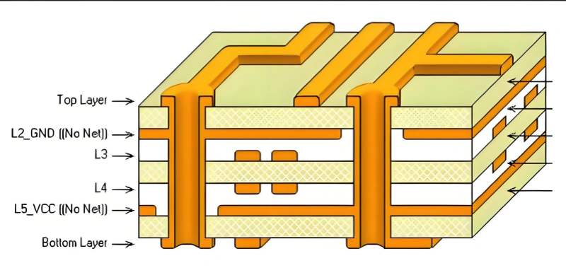
Sobald die Anzahl der Lagen feststeht, besteht die nächste Aufgabe darin, die Reihenfolge dieser Lagen anzuordnen. Die Abbildungen 8-35 und 8-36 zeigen übliche Stapelungen für 4-Lagen- und 6-Lagen-Platinen.

6. Stackup-Analyse
Wie wird gestapelt? Welcher Stackup ist besser? Befolgen Sie diese Grundregeln:
Machen Sie die Bauteilseite und die Lötseite nach Möglichkeit zu vollen Masseflächen (das gibt Abschirmung).
Vermeiden Sie so weit wie möglich benachbarte parallele Routing-Ebenen.
Legen Sie alle Signalebenen nach Möglichkeit neben eine Grundplatte.
Legen Sie kritische Signale neben eine Masseebene und vermeiden Sie es, geteilte Bereiche zu kreuzen.
Wenden Sie diese Regeln auf die in den Abbildungen 8-35 und 8-36 gezeigten allgemeinen Stapelungsbeispiele an. Die Analyse sieht folgendermaßen aus.
(1) Tabelle 8-1 vergleicht die Vor- und Nachteile dreier gängiger 4-lagiger Leiterplattenaufbauten.
| Schema | Schema-Diagramm (ASCII-Art) | Vorteile | Benachteiligungen |
|---|---|---|---|
| Schema 1 | ┌─────────────────────┐ │ PWR01 (Power) │ ├─────────────────────┤ │ SIN02 (Signal) │ ├─────────────────────┤ │ SIN03 (Signal) │ ├─────────────────────┤ │ GND04 (Masse) │ └─────────────────────┘ | Dieses Schema ist in erster Linie darauf ausgelegt, eine einlagige Abschirmung zu erreichen, bei der die Leistungsebene auf der oberen und die Masseebene auf der unteren Lage liegt. | (1) Die Stromversorgungs- und die Masseebene sind zu weit voneinander entfernt, was zu einer übermäßigen Impedanz in der Stromversorgungsebene führt;(2) Die Stromversorgungs- und die Masseebene sind aufgrund des Einflusses von Bauteilanschlüssen und anderen Faktoren sehr unvollständig;(3) Die unvollständige Bezugsebene führt zu diskontinuierlichen Signalbahnen, was es schwierig macht, die erwartete Abschirmwirkung zu erzielen. |
| Schema 2 | ┌─────────────────────┐ │ SIN01 (Signal) │ ├─────────────────────┤ │ GND02 (Masse) │ ├─────────────────────┤ │ PWR03 (Leistung) │ ├─────────────────────┤ │ SIN04 (Signal) │ └─────────────────────┘ | Unter der Komponentenseite befindet sich eine Grundplatte, die sich für Szenarien eignet, bei denen die Hauptkomponenten auf der obersten Ebene platziert sind oder wichtige Signale auf der obersten Ebene verlegt werden. | / |
| Schema 3 | ┌─────────────────────┐ │ SIN01 (Signal) │ ├─────────────────────┤ │ PWR02 (Leistung) │ ├─────────────────────┤ │ GND03 (Masse) │ ├─────────────────────┤ │ SIN04 (Signal) │ └─────────────────────┘ | Ähnlich wie Schema 2 eignet es sich für Szenarien, bei denen die Hauptkomponenten auf der unteren Ebene platziert oder die wichtigsten Signale auf der unteren Ebene geleitet werden. | / |
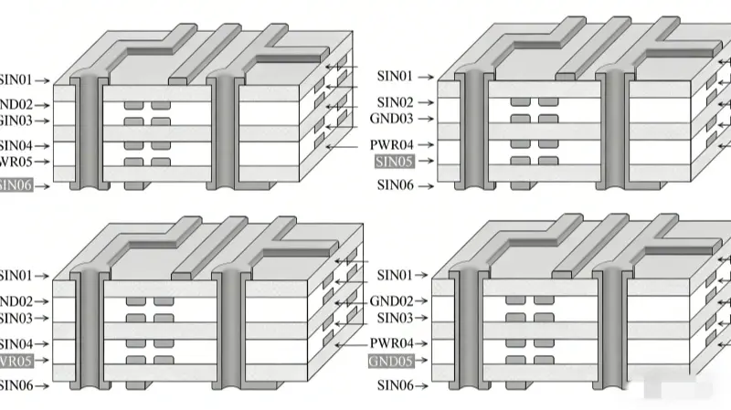
(2) Tabelle 8-2 vergleicht die Vor- und Nachteile von vier gängigen 6-Lagen-Platinenaufbausystemen.
| Schema | Schema-Diagramm (ASCII-Art) | Vorteile | Benachteiligungen |
|---|---|---|---|
| Schema 1 | ┌─────────────────────┐ │ SIN01 (Signal) │ ├─────────────────────┤ │ GND02 (Masse) │ ├─────────────────────┤ │ SIN03 (Signal) │ ├─────────────────────┤ │ SIN04 (Signal) │ ├─────────────────────┤ │ PWR05 (Leistung) │ ├─────────────────────┤ │ SIN06 (Signal) │ └─────────────────────┘ | Mit 4 Signallagen und zwei internen Stromversorgungs-/Masse-Lagen werden mehr Signallagen bereitgestellt, um das Routing zwischen den Komponenten zu erleichtern. | (1) Die Stromversorgungsebene und die Masseebene sind zu weit voneinander entfernt, was zu einer unzureichenden Kopplung führt;(2) Die Signallagen SIN03 und SIN04 werden hauptsächlich auf den Oberflächenlagen verlegt, was zu einer schlechten Signalisolierung und zu Übersprechen führt und eine versetzte Verlegung erforderlich macht. |
| Schema 2 | ┌─────────────────────┐ │ SIN01 (Signal) │ ├─────────────────────┤ │ SIN02 (Signal) │ ├─────────────────────┤ │ GND03 (Masse) │ ├─────────────────────┤ │ PWR04 (Power) │ ├─────────────────────┤ │ SIN05 (Signal) │ ├─────────────────────┤ │ SIN06 (Signal) │ └─────────────────────┘ | Die Leistungsebene und die Grundplatte sind vollständig gekoppelt. | Benachbarte Schichten von Oberflächensignalschichten sind auch Signalschichten, was zu schlechter Signalisolierung und Übersprechen führt. |
| Schema 3 | ┌─────────────────────┐ │ SIN01 (Signal) │ ├─────────────────────┤ │ GND02 (Masse) │ ├─────────────────────┤ │ SIN03 (Signal) │ ├─────────────────────┤ │ GND04 (Masse) │ ├─────────────────────┤ │ PWR05 (Leistung) │ ├─────────────────────┤ │ SIN06 (Signal) │ └─────────────────────┘ | (1) Die Stromversorgungsebene und die Masseebene sind vollständig gekoppelt;(2) jede Signallage grenzt direkt an die interne Stromversorgungs-/Masseebene, wodurch eine wirksame Isolierung von anderen Signallagen erreicht und das Übersprechen reduziert wird;(3) die Signallage SIN03 grenzt an zwei interne Ebenen (GND02 und PWR05), wodurch externe Störungen auf SIN03 und das Übersprechen von SIN03 auf andere Lagen wirksam abgeschirmt werden können. | / |
| Schema 4 | ┌─────────────────────┐ │ SIN01 (Signal) │ ├─────────────────────┤ │ GND02 (Masse) │ ├─────────────────────┤ │ PWR03 (Leistung) │ ├─────────────────────┤ │ GND04 (Masse) │ ├─────────────────────┤ │ PWR05 (Strom) │ ├─────────────────────┤ │ SIN06 (Signal) │ └─────────────────────┘ | (1) Die Stromversorgungsebene und die Masseebene sind vollständig gekoppelt;(2) jede Signallage grenzt direkt an die interne Stromversorgungs-/Masseebene, wodurch eine wirksame Isolierung von anderen Signallagen erreicht und das Übersprechen reduziert wird. | / |
Vergleicht man die Schemata 1 bis 4, so sind die Schemata 3 und 4 eindeutig besser als die ersten beiden Schemata, wenn die Signalleistung die höchste Priorität hat. Im realen Produktdesign sind jedoch die Kosten ein wichtiges Anliegen. Bei hoher Routing-Dichte wählen Designer oft Schema 1 für Stackup, um Kosten zu sparen. Beim Routing nach Schema 1 sollten Sie besonders auf die Kreuzungen zwischen zwei benachbarten Signalschichten achten und versuchen, das Übersprechen so weit wie möglich zu reduzieren.
(3) Für übliche 8-Lagen-Platten sind die empfohlenen Stapeloptionen in Abbildung 8-37 dargestellt. Bevorzugen Sie Option 1 oder Option 2. Option 3 ist brauchbar.

7. Hinzufügen und Bearbeiten von Layern
Wie fügen Sie in Altium Designer Schichten hinzu, nachdem Sie den Stackup-Plan bestätigt haben? Es folgt ein einfaches Beispiel.
Rufen Sie den Menübefehl “Konstruktion → Ebenenstapelmanager” auf oder drücken Sie den Hotkey “DK”, um den Ebenenstapelmanager zu öffnen. Stellen Sie die entsprechenden Parameter wie in Abbildung 8-38 gezeigt ein.
Klicken Sie mit der rechten Maustaste und wählen Sie “Ebene oben einfügen” oder “Ebene unten einfügen”, um eine Ebene hinzuzufügen. Sie können eine positive Ebene oder eine negative Ebene hinzufügen. Verwenden Sie “Ebene nach oben verschieben” oder “Ebene nach unten verschieben”, um die Reihenfolge der hinzugefügten Ebenen anzupassen.
Doppelklicken Sie auf den Ebenennamen, um ihn umzubenennen. Sie können die Layer TOP, GND02, SIN03, SIN04, PWR05, BOTTOM, usw. nennen. Altium Designer 19 unterstützt diese Benennung “Buchstabe + Layer-Nummer”. Dies erleichtert das Lesen und Erkennen.
Stellen Sie die Platten- und Lagenstärke entsprechend der Stapelung ein.
Um die 20H-Anforderung des Musters zu erfüllen, können Sie den Sperrbetrag der negativen Ebene (innerer Versatz) einstellen. [Hinweis: Im Originaltext wird “20H” verwendet. Der Übersetzer behält diesen Begriff bei].
Klicken Sie auf “OK”, um die Stackup-Einstellungen zu beenden. Ein Beispiel für den Stapelungseffekt einer 4-Lagen-Platine ist in Abbildung 8-39 dargestellt.

8. Empfehlung
Es wird vorgeschlagen, Signallagen als positive Ebenen und Leistungs- und Masselagen als negative Ebenen zu behandeln. Dieser Ansatz kann die Dateigröße erheblich reduzieren und die Entwurfsarbeit beschleunigen.