
HDI PCB Capabilities
FLJ PCB supports HDI boards with microvias, build-up layers and fine routing. Review construction and drilling together when planning dense component escapes.
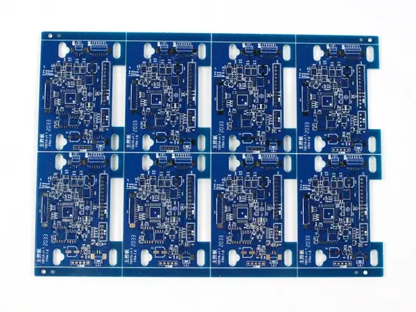
High-density interconnect for dense routing
HDI uses fine features and microvias where a through-hole layout cannot provide the required connection density.
Build-up layers connect component pads to inner routing without carrying every via through the full board thickness. This supports dense devices and compact assemblies. Construction follows pad geometry, layer transitions and electrical requirements.
FLJ publishes general HDI constructions and a specialist table with different scopes. Engineering review connects geometry to laminate and process sequence rather than treating every minimum as interchangeable.
Specialist HDI process range
Published process ranges are matched to your material and construction during engineering review.
Copper weight, geometry and laminate affect the process window. Impedance targets belong to a defined stack-up and trace geometry; the tolerance does not substitute for this information.
| Merkmal | Published capability |
|---|---|
| Schichten | 1–32 |
| Listed ELIC structure | 5+2+5 |
| Core thickness | 0.05–1.5 mm |
| Finished thickness | 0.3–3.5 mm |
| Minimum laser hole | 0.075 mm |
| Minimum mechanical hole | 0,15 mm |
| Minimum line / space | 0.030 / 0.030 mm |
| Copper foil | 0.5–5 oz |
| Maximum processing size | 700 × 610 mm |
| Layer registration | ±0.05 mm |
| Outline tolerance | ±0.075 mm |
| Impedance tolerance | ±8% |
Build-up structures and via choices
The general FLJ table lists 1+n+1, 1+1+n+1+1, 2+n+2 and 3+n+3 structures.
These describe build-up layers around a central structure. Design transitions determine where blind, buried or through vias are useful. Sequential lamination and via arrangements affect complexity, schedule and process review.
Laser blind vias can be plated and filled within the published scope. Via-in-pad needs suitable filling and final pad surfaces because the feature becomes part of component soldering. Identify stacked or staggered arrangements in the construction data so the route matches the intended interconnect.
Drilling follows material and construction
Laser microvias and mechanical holes perform different manufacturing tasks.
The general table lists 0.10–0.15 mm laser holes; the specialist table lists a 0.075 mm minimum. These are separate ranges. Hole diameter, dielectric thickness and via depth must be reviewed together.
FLJ specifies mechanical blind or buried drilling, controlled-depth drilling and backdrilling for ceramic-material and PTFE high-frequency hybrid processes, rather than laser drilling. A material name on a broad list does not establish laser-microvia compatibility for that construction.
Microvia pads and construction conditions
Small feature values work as a construction. We review the stackup, via geometry and component escape together rather than combining unrelated minimums.
| Merkmal | Process reference | How it applies |
|---|---|---|
| Laser capture-pad reference | 10 mil pad for a 4 mil hole; 11 mil for a 5 mil hole | General laser-hole table; not the pad limit for every specialist microvia |
| Build-up sequence | Reviewed with layer arrangement and via span | Separate the dielectric depth, land and fill for each stage |
| Via fill and pad finish | Connect filling with the intended device pad | Review resin or copper-fill route and surface preparation |
| Registration | Match the published tolerance to the selected construction | Routing escapes and capture-pad allowances are reviewed together |
Review routing and assembly together
Send current board data, proposed stack-up and open construction questions.
Dense component escapes need suitable pad geometry, solder-mask openings and paste preparation. Signal requirements should identify reference layers and impedance goals. Electrical test access and assembly inspection are useful early planning topics.
Our engineers follow up on drilling, filling, transitions and materials needed for manufacture. Start the discussion before every choice is final. Revision identification keeps the agreed board and assembly information connected for production.
Frequently asked questions
Is every multilayer board HDI?
No. Multilayer describes conductive layers. HDI adds dense interconnect features such as laser microvias and build-up structures.
Can I combine every minimum?
The usable combination follows copper, dielectric thickness, laminate and via structure, reviewed together.
Can you review an unfinished stack-up?
Yes. Send current layout, component escape and signal goals. We can discuss construction and remaining fabrication information.
Explore related capabilities
Let’s review your next build
Send your available board files, drawings or project questions. Our team will review the information and follow up with you about the next step.