
LASER MICROVIA FABRICATION
Microvia PCB
Valmistus
Small connections. More room for your circuit.
FLJ manufactures microvia PCBs with laser-formed interconnections, copper filling and stacked or staggered build-up structures. From prototype boards to production, the hole geometry, copper interface and finished landing are made as parts of one construction.
Get a Microvia PCB Quote
Explore microvia manufacturing
THE CONNECTION, DIMENSION BY DIMENSION
Microvia Geometry and Fabrication Capabilities
A microvia is a shallow interlayer connection formed to a copper landing beneath a build-up dielectric. Its opening, depth and surrounding lands work together: a small hole still needs room for registration and a sound copper connection.
Hole Opening and Landing Geometry
The capture land surrounds the opening at the entry layer. The target land is the copper at the bottom of the hole. Between them, the laser-formed opening typically narrows toward the target, exposing dielectric along the wall and copper at the landing.
These are separate features. The opening describes the entrance, the target defines where the new copper must join the existing circuit, and the land sizes provide the surrounding copper area. A hole diameter alone does not describe that complete connection.
Matching Hole Diameter to Dielectric Depth
Aspect ratio relates the processed depth to the specified hole diameter. For the same depth, reducing the diameter increases that ratio and changes access for cleaning and copper deposition. At the board surface, the device pitch and fan-out pattern limit the available land area. Diameter, depth and pad space therefore need to be selected together.
Connection depth / opening diameter. These illustrative dimensions show the calculation; the fabrication dimensions belong to the selected build.
FLJ’s laser-hole references pair a 4 mil hole with a 10 mil pad and a 5 mil hole with an 11 mil pad. Read each hole and pad as a pair. The pad column is the published pairing reference; the individual capture and target lands are dimensioned in the actual construction.
Scroll to view all columns.
| Laser hole | Paired pad | Metric equivalent: hole / pad |
|---|---|---|
| 4 miljoonaa | 10 mil | 101.6 / 254 µm |
| 5 miljoonaa | 11 mil | 127 / 279.4 µm |
1 mil = 25.4 µm. See the PCB manufacturing capabilities for the wider fabrication range.
Hole spacing: the same-net laser-hole wall-to-wall clearance reference is 6 mil (152.4 µm), measured between hole edges. Centre-to-centre pitch also includes the hole dimensions.
Sequential build-up: our laser build-up reference covers 1–5 stages, with each stage mapped to the dielectric and via sequence of the complete board.
CHOOSE THE COPPER PATH
Microvia Connection Options
A single-level microvia connects one build-up layer to its target below. When the circuit needs another connection level, the position of the next microvia determines how the copper path continues through the intermediate layer.
Stacked and Staggered Microvias
In a stacked construction, successive microvias align vertically. The upper connection lands on the prepared copper over the filled lower microvia. In a staggered construction, the upper connection lands at an offset position and reaches the lower microvia through the intermediate copper pattern.
A vertical landing over the filled lower connection.
A separate landing linked through the intermediate pattern.
Stacking can reduce the lateral area occupied by the interconnection. Staggering gives the intermediate connection a separate landing and uses routing space between the holes. The choice depends on the package escape, land geometry, materials, filling and verification of the selected construction. The wider HDI PCB service explains how these features fit into the complete build-up.
Microvia-in-Pad
Microvia-in-pad places the connection inside a component land. It is a placement choice that can be used with different interconnection arrangements, rather than a separate alternative to stacked or staggered microvias.
Moving the connection into the pad can free space otherwise needed for a short fan-out trace and a separate via land. In a filled in-pad construction, deposited copper occupies the opening and supports the overlying copper land. Preparing that surface and applying the selected finish provides the component-attachment surface while retaining the interlayer path. FLJ combines the fabrication with PCB-kokoonpano when a project needs populated boards.
FROM AN OPENING TO A COPPER CONNECTION
Microvia Manufacturing: Laser Drilling and Copper Filling
FLJ carries the microvia through hole formation, surface preparation, copper deposition and the required finishing operations. Each stage establishes the surface or copper geometry needed by the next.
Laser Opening and Target-Land Preparation
The starting build-up presents an entry copper structure and dielectric above the intended target land. Depending on the material and laser route, an opening in the entry copper may be prepared before the underlying dielectric is removed. The laser then forms the recess to the intended target copper. Energy and exposure are controlled to remove the dielectric while preserving that landing.
Hole preparation then removes residue from the recessed surface and exposes the target for the next copper connection. Residue remaining between the deposited copper and the target can interrupt their bond. Cleaning the hole bottom therefore belongs to making the interconnect, rather than being only a cosmetic treatment of the opening.
Metallization and Copper Filling
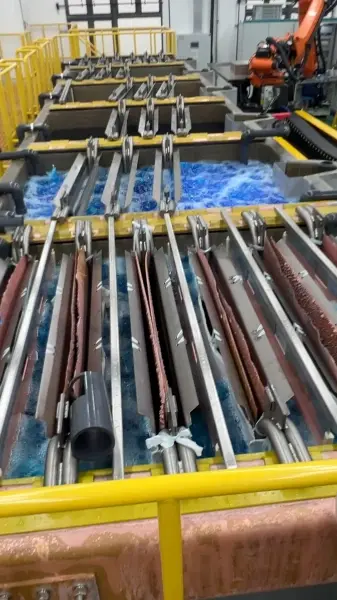
The exposed dielectric wall first needs a conductive surface. Metallization establishes that surface, and subsequent copper deposition builds the connection to the target land. Wetting and solution exchange help the process reach the recessed surfaces; the mouth and bottom do not receive material under identical conditions.
Copper filling adds another objective: developing the deposit inside the microvia to create the specified filled structure. An opening that has closed over can still contain a void, so external appearance alone does not describe the internal copper. The hole profile, deposited copper and resulting top surface are assessed as one feature.
Preparing the Next Landing or Assembly Pad
A filled microvia can become the foundation for the next connection. The copper above the lower feature must provide the intended landing geometry and a prepared interface for the upper microvia. In a finished in-pad land, the surface instead supports component attachment.
Surface finish protects exposed copper and provides the selected assembly surface. It does not replace the copper connection inside the hole. Copper filling, resin filling used in other via constructions, and the final finish are separate operations with different jobs.
VERIFY THE STRUCTURE THAT WAS BUILT
Microvia Interfaces and Reliability Verification
A useful inspection result corresponds to the actual layer pair, copper interface and connection arrangement. FLJ links the specified construction to the appropriate manufacturing checks and verification records.
Interfaces Within the Copper Connection
The deposited copper meets the target land at the bottom of each microvia. In an aligned multi-level connection, an additional junction forms where the upper microvia meets the copper over the lower one. The copper around the mouth is another part of the current path. These locations have different geometries even when the completed network passes an initial continuity test.
Matching Verification to the Actual Structure
A prepared microsection reveals the local shape, copper fill and interfaces in the cut plane. PCB electrical testing checks continuity and isolation of the specified network. These checks establish different kinds of evidence: a section shows one physical plane, while the network test describes the connections at its test conditions.
For qualification that requires thermal and electrical observation, a coupon can connect representative microvias in a series chain. A discontinuity in that chain changes its electrical response, allowing the connection to be observed during the defined heat exposure. The coupon identifies the layer pairs, stack arrangement and material system represented.
A weak interface may open on heating and close after cooling. Monitoring during exposure can reveal behavior that an ambient reading misses. Keeping the exposure and resistance record with the chain construction makes that result interpretable for the board being qualified.
Scroll to view all columns.
| Observation | What it examines | What the record identifies |
|---|---|---|
| Microsection | Local geometry, fill and copper interfaces in the prepared plane | Section location, represented feature and build revision |
| Continuity and isolation | The electrical path and separation of the specified network | Tested network, conditions and result |
| Applicable thermal / electrical verification | Electrical response of a representative interconnect during defined exposure | Chain construction, exposure, monitored quantity and acceptance criterion |
The thermal profile, observation method and acceptance conditions follow the qualification requirement for the selected construction. A test name alone does not establish that the coupon represents the production microvia.
PROTOTYPE TO PRODUCTION
Bring the microvia construction into your next board build. Send the layer stack, via arrangement and quantities for a fabrication quotation.