
















OSP vs ENIG: Choose a PCB Surface Finish for SMT, Storage and Rework
OSP and ENIG can both provide planar solder pads for SMT, but they protect the copper in different ways. OSP uses a thin organic coating over copper and is often attractive when cost and a prompt, controlled assembly route matter. ENIG puts electroless nickel and immersion gold over the copper and often gives more process latitude for storage, handling and multi-stage assembly, at higher finish cost. The choice should follow the actual build and logistics plan rather than a blanket claim that one finish makes better solder joints.
Philifast offers separate OSP a ENIG information pages. This comparison helps connect those finish descriptions to the assembly schedule and product needs. For a different comparison, see Philifast’s ENIG versus HASL guide.
First understand what reaches the solder pad
OSP forms an organic protective film directly on the exposed copper. During soldering, the process is designed so that solder wets the underlying copper. ENIG has a nickel barrier with a thin gold layer over it; soldering consumes or displaces the surface gold and the joint forms through the finish system. Sharretts Plating’s OSP/ENIG comparison describes the constructions and their manufacturing implications. Exact finish thickness and acceptance limits belong in the fabrication specification, not a generic article.
This explains why planarity alone is not the deciding factor. Both finishes follow the underlying pad geometry and avoid the uneven solder coating of hot-air leveling, but their surfaces encounter paste, handling and heat differently. For a fine-pitch or BGA design, check pad geometry, stencil, component coplanarity and solder process as well as finish. Selecting ENIG cannot repair a poor land pattern, and OSP is not automatically disqualified by pitch alone.
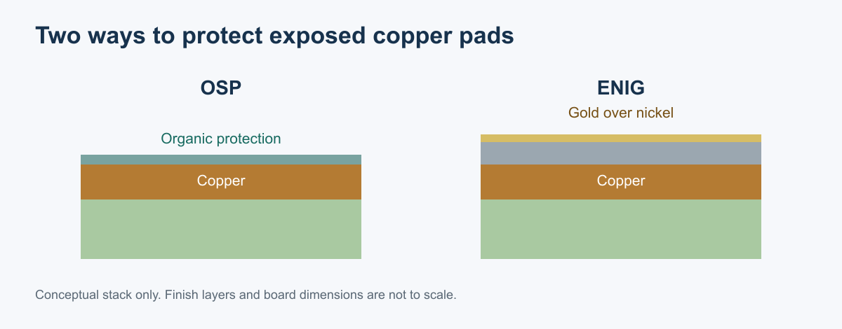
Illustration: Layer relationship only; thicknesses are intentionally not to scale.
Compare the job, not just the coating
| Project condition | OSP consideration | ENIG consideration |
|---|---|---|
| Fine-pitch SMT pad planarity | Provides a flat surface when the underlying board is well made. | Also provides a planar surface; no need to choose ENIG solely because the board is fine pitch. |
| Rapid board-to-assembly flow | Often a good fit when handling and storage are controlled. | Works too, but its higher finish cost may bring little benefit for this condition alone. |
| Long or uncertain storage and shipping | Requires careful shelf-life and handling control; confirm the fabricator’s approved window. | Often chosen for greater storage/handling latitude; still requires proper packaging and inspection. |
| Several soldering stages or expected rework | Additional heat and exposure can reduce OSP margin; confirm the real sequence. | May offer more flexibility, but repeated heating is still a product/process issue. |
| Exposed contact or wire-bond requirement | Check whether an organic-coated copper surface is appropriate for the actual contact. | ENIG is not a universal substitute for hard contact gold or a specified wire-bondable finish; qualify the interface separately. |
| Finish cost | Commonly lower. | Commonly higher due to nickel/gold processing; compare a complete quote. |
JLCPCB’s finish comparison highlights OSP’s process and rework considerations. These are tendencies, not universal rules. The actual outcome depends on coating process quality, pad design, packaging, handling, solder paste, thermal profile and the time between fabrication and assembly.
Three common board routes make the trade-off more concrete:
- Boards fabricated and assembled promptly at one site: OSP can be a sensible candidate if the chosen OSP process, packaging and thermal route are approved; ENIG remains an option when another requirement calls for it.
- Boards shipped internationally and held for an uncertain build date: ENIG’s metallic protection may offer more scheduling latitude. The actual shelf-life acceptance is still set by the fabricator’s process and storage instructions, not a generic month count.
- Double-sided SMT plus later selective solder or expected repair: Identify which pads remain unsoldered after each heat excursion. Ask both suppliers to evaluate whether their chosen OSP chemistry retains an adequate solderability window, or whether ENIG better fits that sequence.
The deciding variable can be a small set of pads, rather than the whole board. If only a few exposed contacts have a distinct requirement, discuss selective finish or a separate contact construction with the fabricator. That introduces its own process and cost questions; do not assume mixed finishes are available on a quoted design.
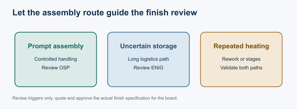
Illustration: These are review triggers; engineering approval determines the final finish.
Two decisions that prevent avoidable rework
Map the full thermal route. List the number and sequence of soldering, selective solder, repair or other heating operations, including whether the board is populated on both sides. Do not interpret “OSP supports one reflow” or “ENIG supports unlimited reflow” as a universal fact. Ask the fabricator and assembler whether the specified finish remains suitable for the actual sequence and storage between steps.
Ask specifically about unsoldered exposed pads after the first heating step. Soldered joints have already consumed the local finish; later soldering of previously bare pads depends on their condition at that later operation. This is why a two-sided assembly route needs more than the headline number of reflows. Surface condition, handling between operations, flux and thermal profile all affect the outcome.
Control the board’s time and handling. Give the expected shipping path, storage condition and interval before assembly. Avoid touching exposed pads; use the packaging and handling instructions approved for the finished boards. If boards sit longer than planned, agree on how solderability will be evaluated before starting production. A finish selection made for immediate assembly can be undermined by a delayed build.
For traceability, record the fabrication lot, finish type, fabrication and receipt dates, package opening date, storage conditions and assembly date where the project requires them. If an OSP lot exceeds the agreed window or packaging is damaged, hold it for engineering disposition rather than assuming an extra cleaning step will restore it. Cleaning or reworking a finish can change solderability and should follow an approved process. ENIG boards also need controlled handling; visible gold color alone does not prove solderability.
ENIG has its own quality risks if the plating process is not well controlled; it should not be portrayed as a free reliability upgrade. Specify the applicable finish requirements, request fabrication quality evidence as appropriate, and investigate solderability problems rather than assuming the visible gold color proves a sound interface.
One named concern is nickel corrosion during the immersion-gold process, often discussed as “black pad.” It is a fabrication-process failure mode associated with poor solder-joint reliability, not a reason to assume every ENIG board is suspect. Sharretts’ process discussion identifies this risk. If the application is sensitive, ask what finish specification, process control and acceptance evidence will be used. For OSP, ask the corresponding questions about coating, packaging and solderability after the planned storage and heat exposure. The comparison is between controlled processes, not idealized coatings.
Follow the finish through the complete assembly route
The surface finish is chosen before the board is built, but its condition is tested by the downstream schedule. Draw the actual route: board fabrication, shipment, receiving, storage, paste printing, first-side reflow, board turnover, second-side assembly, any additional soldering and final rework. Mark the interval between each step and which pads remain unsoldered at each thermal exposure. A two-sided build can present a different risk from one prompt reflow because exposed pads may see additional handling or heat before they are used.
For OSP, confirm the manufacturer’s process-specific handling and storage guidance for the ordered finish and packaging. Do not take a generic internet shelf-life figure as approval for an unknown OSP chemistry, board package or environment. For ENIG, confirm that the selected finish specification and fabrication lot documentation match the order; ENIG’s layered structure does not eliminate the need to control process quality or investigate a suspect joint. In either case, ask how a delayed or opened package will be assessed before assembly begins.
The choice often changes with the logistics case. If fabrication and SMT are scheduled close together, packaging remains controlled and only the planned solder cycles occur, OSP may meet the actual process need without paying for finish properties that the design does not use. If storage duration is uncertain, boards require more handling, or exposed lands must remain available for another operation, ENIG may be worth evaluating for its different surface and assembly behavior. Neither scenario is a guarantee: use the fabricator’s documented process and the assembly route to qualify the choice.
For a product with variants, compare the actual pad use rather than treating the board as one uniform surface. Some versions may leave connector, test or spare pads unsoldered while others populate them. Those exposed pads can experience a different handling and rework history from soldered component lands. Identify which exposed features matter for later assembly, service or test and make sure the finish evidence covers them.
The evidence should answer a specific question. A solderability or surface-finish inspection may support a decision about board condition; a good SPI result only describes the paste deposit and cannot verify the board finish. A completed solder joint should be judged using the agreed assembly criteria. If a rework procedure adds thermal cycles or exposes previously unsoldered pads, validate that operation on the actual construction and process instead of assuming the original finish decision covers every later repair.
Specify the finish standard and its scope
Name the finish on the fabrication drawing and purchase order, and state the revision that governs it. As of September 29, 2026, IPC’s revision table lists IPC-4552B for electroless nickel/immersion gold and IPC-4555 as the performance specification for high-temperature organic solderability preservatives. IPC-4555’s published scope should not be generalized to every OSP chemistry or process. Check the current IPC revision table and confirm that the selected document fits the ordered finish.
Where the project relies on thickness, appearance, solderability, storage or test criteria, state the applicable requirement and evidence source rather than assuming the finish name alone defines it. Tie the fabrication lot, finish revision and receipt record to the assembly build. If a standard revision is frozen in an existing design, change it through engineering change control instead of allowing a quote to silently substitute a newer or different specification.
Rework deserves its own boundary. Removing a component can heat nearby pads and leave flux, solder or surface damage; cleaning, dressing or applying new solder can create another condition that the original board-finish purchase did not qualify. Agree whether rework is allowed, which instructions control it, how the repaired joint is inspected, and whether a previously unused pad can be reused after the local process. If repeated repair is likely, validate representative coupons or assemblies through the intended sequence and retain the result against the exact finish and board revision.
Do not assign a fixed number of acceptable reflows to OSP or ENIG from a generic comparison chart. The outcome depends on the finish chemistry, vendor controls, solder alloy and flux, thermal profile, handling and the condition of the specific pads. Ask for the product-specific finish data and process review; then put the agreed number of assembly operations, if controlled, into the project plan rather than presenting a blog rule as a supplier guarantee.
If the finish changes between board revisions, treat it as a controlled material change. Review pad geometry, solder-mask openings, any exposed gold fingers or connector contacts, downstream storage and all operations that use an unsoldered copper land. Update the fabrication drawing and assembly traveler together, and preserve the prior finish record for boards already in stock. This avoids mixing boards with different surface histories in one assembly lot just because the product name and outline remained the same.
Do not treat OSP and ENIG as the only possible finish choice in every design. If the real question is whether ENIG’s flatness or storage behavior is needed compared with another finish, use the separate ENIG vs HASL comparison for that decision; this article focuses on OSP versus ENIG through SMT timing, storage and rework.
What to tell Philifast before choosing
Provide component pitch and pad types, assembly location, expected board-to-assembly interval, thermal/rework steps, any contact or bonding surfaces, and the applicable finish specification. Ask Philifast to confirm the proposed finish, packaging and handling plan for that build and to quote both options if the trade-off is material. The best answer is the finish whose process window matches the product’s actual schedule and assembly path.
Request the finish designation on the fabrication drawing and make sure the assembler’s build plan uses the same revision. If a late scheduling change adds months of storage or another soldering step, revisit the finish decision before ordering more boards. That change may be cheaper to handle in the board specification than through solderability troubleshooting after material arrives.