


Introduction: Why Understanding PCB and PCBA Matters
Every electronic device you use relies on a Trykt kredsløb (PCB) as its physical foundation. Think of a bare PCB as a blank canvas—a rigid board with copper traces but no components. PCB-samling (PCBA) transforms that canvas into a functional masterpiece by mounting and soldering all necessary components.
The distinction between PCB and PCBA is one of the most critical concepts in electronics manufacturing, yet these terms are often confused. A bare board cannot power your product; only a fully assembled PCBA brings it to life.
This article clarifies exactly what separates them, why the difference matters for your project’s cost and quality, and how each stage fits into the broader production workflow. You’ll discover how design choices, assembly methods, and testing ensure reliability in everything from simple gadgets to complex industrial systems.
What is a PCB? The Foundation of Modern Electronics
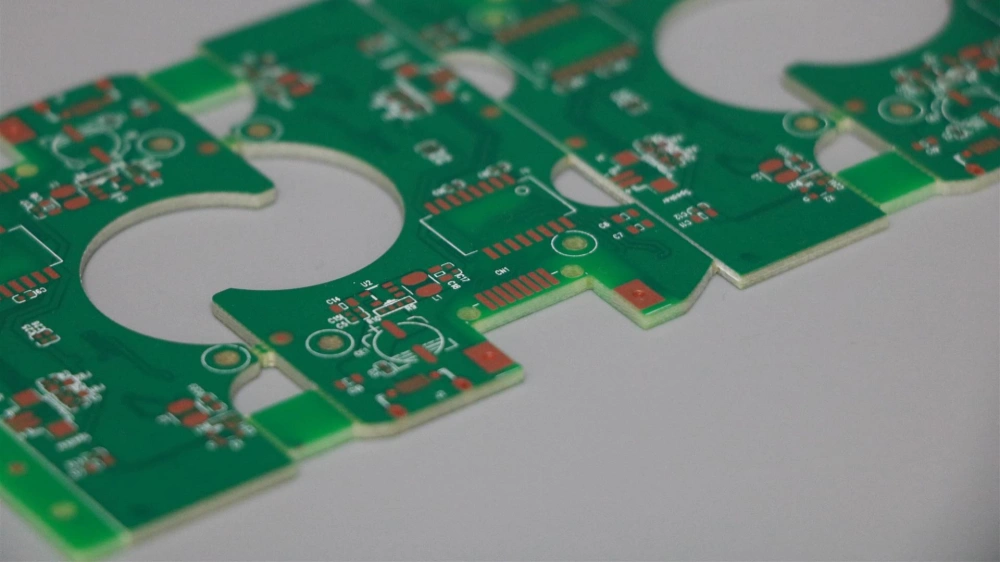
At the core of every electronic device is a printed circuit board (PCB). This flat, rigid board serves as the physical platform that mechanically supports and electrically connects electronic components. The base material, known as the substrate, is typically made of fiberglass-reinforced epoxy resin (FR-4), which provides insulation and structural strength.
On this substrate, thin sheets of copper foil are laminated and then etched away, leaving behind a precise network of Kobberspor. These traces act as wires, routing power and signals between components exactly where needed.
A PCB can be single-sided, with one copper layer, or multi-layered, stacking several copper sheets separated by insulating material. Multi-layer PCBs allow for far more complex routing in a compact space. Tiny plated holes called vias connect traces between layers.
Beyond simple connectivity, the board also manages heat dissipation and reduces electromagnetic interference. In short, the PCB transforms a pile of discrete parts into a functional, reliable system, defining how each component interacts before assembly even begins.
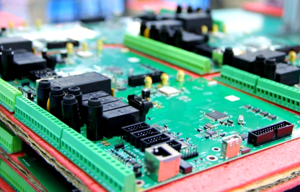
What is PCBA? Bringing the Board to Life
Before assembly, a bare PCB is like an empty canvas—just conductive tracks without purpose. The transformation happens during PCB-samling, where electronic components are placed and soldered onto the board to create a functional circuit. The finished product is called PCBA (Printed Circuit Board Assembly). This is the stage where a design actually comes to life.
The assembly process relies on two core techniques:
- SMT (Surface-Mount Technology): Components are mounted directly onto the board’s surface. It supports miniaturization and high-speed automated placement, making it the dominant method in modern electronics.
- Through-hole technology: Component leads are inserted into drilled holes and soldered to pads on the opposite side. It delivers stronger mechanical bonds, ideal for connectors or components that face physical stress.
Most real-world products use a hybrid approach, combining SMT for efficiency and through-hole for durability where needed. The key distinction is simple: a bare PCB is a static platform, while a PCBA is a fully functional electronic assembly ready for integration and testing.
PCB vs PCBA: Key Differences at a Glance
At a glance, the distinction between a bare board and an assembled board shapes everything from procurement to performance. The table below breaks down the five critical areas where PCB and PCBA diverge.
| Aspekt | PCB (Bare Board) | PCBA (Assembled Board) |
|---|---|---|
| Definition | A bare substrate of insulating layers and copper traces without any electronic parts. It is the physical canvas for a circuit. | A complete, functional assembly where all components have been soldered onto the PCB. It is the active electronic module. |
| Components | Contains only conductive pathways, pads, vias, and solder mask. No active or passive electronic parts included. | Populated with ICs, resistors, capacitors, connectors, and all other electronic components required for operation. |
| Core Function | Provides structural support and electrical routing between component locations. | Executes the intended electronic function: processing signals, distributing power, and running device firmware. |
| Manufacturing Focus | Etching, drilling, plating, and solder mask application. | Solder paste printing, component placement, reflow soldering, and post-assembly testing. |
| Cost Structure | Cost driven by layer count, board size, material grade, and surface finish. | Cost includes bare PCB, component procurement, assembly labor, and testing; components often make up 60–80% of total cost. |
The PCB Manufacturing Process: From Design to Fabrication
Den PCB-fremstilling process translates digital design files into physical bare boards. It starts with a design for manufacturability (DFM) review to validate stackups, trace clearances, and drill sizes against production capabilities.
Next, photolithography transfers the circuit pattern onto copper-clad laminate. A chemical etching process removes unwanted copper, leaving precise copper traces and pads. Precision drilling creates via holes and mounting points, followed by copper plating to establish electrical connections between layers.
A solder mask layer is applied over the entire board, exposing only the pads needed for soldering. A surface finish—such as ENIG, HASL, or OSP—protects exposed copper from oxidation and improves solderability.
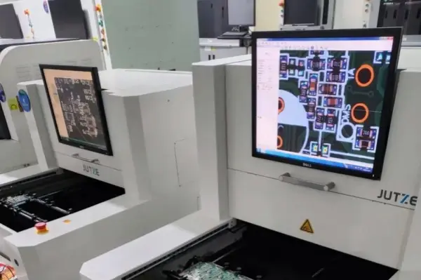
Finally, every board undergoes automatiseret optisk inspektion (AOI) to catch shorts, opens, or trace defects, followed by electrical testing (flying probe or bed-of-nails) to verify full connectivity before shipment.
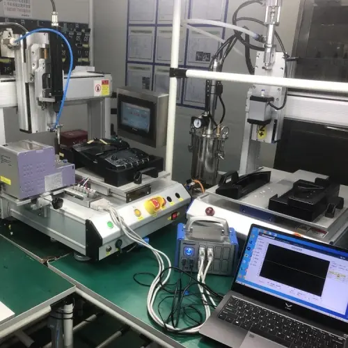
The PCBA Process: How Components Are Mounted and Soldered
The heart of the PCBA process lies in precisely mounting and soldering components to the bare board. For most modern electronics, this begins with SMT-montering. A solder paste stencil aligns with the board’s pads, and a precision machine deposits tiny amounts of paste. High-speed pick-and-place systems then position surface-mount components onto the paste with remarkable accuracy.
Once all parts are set, the boards move through a reflow soldering oven. Controlled heat profiles melt the solder paste, form solid joints, and then cool the assembly without thermal shock. This single pass secures hundreds of miniature components in seconds.
Not every component can survive the reflow temperatures. Larger connectors, transformers, or through-hole parts require a different approach. These are added using THT assembly, where component leads are inserted into drilled holes. The board then passes over a wave soldering machine, which applies molten solder to the bottom side, filling each hole and anchoring the leads.
Verification follows immediately. Automated optical inspection (AOI) cameras scan every joint for missing parts, bridging, or misalignment. For hidden connections—such as those under ball grid array (BGA) packages—X-Ray inspection reveals internal solder quality without physical contact.
Advanced Testing and Quality Control in PCB and PCBA Production
Beyond initial visual checks, a rigorous sequence of electrical and environmental tests confirms every board meets design and reliability requirements. In-circuit testing (ICT) verifies individual component placement, values, and basic solder joint integrity by probing test points across the bare assembly. It catches missing parts, wrong resistors, or shorts before functional checks begin.
Functional testing (FCT) then simulates real operating conditions—powering the unit and running signals through it—to prove the board does exactly what it was designed to do.
Solder paste inspection (SPI) operates earlier in the line, scanning paste deposits immediately after printing. It measures height, volume, and alignment, stopping defects like insufficient solder or bridging before components are placed. For hidden joints under BGAs or QFNs, X-ray provides the only non‑destructive window into internal fillet quality and void levels.
Long‑term reliability testing subjects samples to thermal cycling, vibration, and burn‑in to uncover latent weaknesses. Throughout every stage, adherence to IPC-standarder provides a shared language for acceptable workmanship and defect classification.
This structured kvalitetskontrol chain—from SPI and ICT through FCT and environmental stress—ensures each PCB and PCBA shipment performs flawlessly in the field, not just on the test bench.
Choosing the Right Partner for Your PCB and PCBA Needs
A reliable supplier evaluation starts well beyond the price sheet; it demands a hard look at certifications and standards. Seasoned buyers prioritize ISO 9001 or IATF 16949 compliance, ensuring the PCB manufacturer operates within a closed-loop quality system. Equally critical is verifying that in-house testing—AOI, X-Ray, and flying probe—exists as a non-negotiable baseline, not a costly add-on.
Beyond compliance, you need a partner whose technical capabilities align with your roadmap. If your project involves mixed-signal designs or high-density layouts, the facility must handle HDI microvias and fine-pitch placement without outsourcing critical steps.
A true one-stop PCBA service provider offers a seamless turnkey solution, consolidating fabrication, BOM sourcing from authorized channels, and final box-build assembly. This approach eliminates the finger-pointing common in multi-vendor chains.
Lead times expose a factory’s planning maturity. An agile PCB manufacturer will offer expedited prototypes within 24-48 hours without sacrificing electrical testing. Finally, scrutinize engineering support. Responsive design-for-manufacturing (DFM) feedback before tooling prevents performance drift.
Case Study: How Turnkey PCB and PCBA Services Accelerate Product Development
A medical device startup approached PHILIFAST with a tight launch deadline. Their design was ready, but they needed to move from a handful of benchtop prototypes to a market-ready batch in under eight weeks. Isolated suppliers had quoted 12 to 16 weeks split across three separate vendors for fabrication, component sourcing, and assembly.
By consolidating the entire project with PHILIFAST’s turnkey PCB and PCBA service, the team cut lead time by nearly 50%. The in-house engineering team performed a full DFM review upfront, resolved three thermal and trace clearance issues before production, and managed end-to-end component sourcing with authorized distributors.
The final batch passed all functional testing and regulatory inspection on the first pass, allowing the startup to launch two weeks ahead of their original schedule.
Frequently Asked Questions About PCB and PCBA
What is the real difference between a PCB and a PCBA?
A bare PCB is the rigid board with copper traces and pads — an empty platform. A PCBA is that same board after components are soldered on, turning it into a functioning electronic circuit. Think of the PCB as a skeleton and the PCBA as the complete organ system.
How is PCB assembly cost typically calculated?
PCB assembly cost depends on three main factors: board complexity (layer count, surface finish), component count and type (fine-pitch BGAs or through-hole parts), and order quantity. Setup charges often dominate small batches, while component material costs drive pricing for larger volumes.
What is the typical lead time for prototype PCB and PCBA?
Standard prototype bare PCBs take 3–5 days for 2–4 layer designs. Adding SMT assembly extends lead time to 7–10 days total. Expedited services can deliver fully assembled prototypes in as little as 48–72 hours for urgent projects.
Conclusion: Mastering PCB and PCBA for Your Next Project
Mastering the distinction between PCB and PCBA is the foundation of a successful electronics manufacturing journey. A bare PCB is the inert skeleton—a canvas of fiberglass and copper traces—while a PCBA is the living, functional assembly where every component pulses with purpose. Overlooking this difference during design or procurement leads to costly miscommunication and prototype delays.
Quality manufacturing transforms this design intent into a reliable product. A well-fabricated board with precise impedance control and a flawless assembly process—from solder paste printing to reflow profiling—ensures your finished PCBA survives thermal stress and real-world operation. Cutting corners on either stage invites field failures that erode trust and inflate lifetime costs.
Whether you’re iterating a prototype or scaling volume production, align yourself with partners who treat both fabrication and assembly as one integrated discipline.
Ready to Get Started with Your PCB and PCBA Project?
Move your PCB and PCBA project from design to delivery with a single partner. Get a full turnkey manufacturing solution—from bare board fabrication to tested, box-build assemblies—all managed under one roof.
PHILIFAST’s engineering support starts with a free design review to flag any production risks before you commit, helping you save time and cost.

