


SMT (overflademonteringsteknologi)
With technology moving forward, chip packaging around the world has shifted from through-hole parts with dual inline leads to surface-mounted packages. Today we will talk about surface mount technology, or SMT. SMT is the most common assembly method in modern electronics.
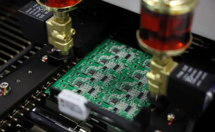
SMT stands for Surface Mount Technology. People also call it surface mount assembly or surface mount mounting. It is a set of processes used in electronics assembly. SMT places components that have no long leads or only short leads onto the surface of a printed circuit board, or other substrates. Those components are usually called SMC or SMD, which means surface mount components. SMT parts are soldered to the board by methods like reflow soldering or wave soldering. This forms a complete circuit assembly.
Compared with older package styles, SMT puts higher demands on chip packaging. Today’s advanced package types include wafer level packaging (WLP), three-dimensional packaging (3DP), and system-in-package (SiP). These types require stricter process control, tighter tolerances, and more advanced manufacturing skills.
What is Wafer Level Packaging (WLP)?
Wafer Level Packaging, or WLP, is an advanced packaging method. WLP has grown fast in recent years. People use it because it makes small packages, gives good electrical performance, helps heat dissipation, and lowers cost.
WLP is different from traditional packaging because the package steps happen while the chips are still on the wafer. A protective layer can be attached to the top or bottom of the wafer. Then the I/O connections are made. After that, the wafer is diced into single chips.
WLP has several clear advantages over older methods.
Small package size.
Because WLP does not need wire bonds, bonding pads, or a plastic mold, the package does not have to extend beyond the die. So the WLP package size is nearly the same as the chip size.High data speed.
WLP usually uses shorter interconnects than traditional wire-bond parts. When the system needs high speed or high frequency, the shorter paths give better signal performance.High connection density.
WLP can use area-array connections, not only edge connections. This lets designers place many more connections per unit area between the chip and the board.Shorter production cycle.
Because the packaging is done at wafer level, the steps from die fabrication to finished packaged part are simpler. This reduces the number of process steps and shortens lead time.Lower process cost.
WLP performs packaging and testing at the wafer level and benefits from batch processing. The cost per device can drop when more good die fit on each wafer. Trends like smaller die sizes and larger wafer diameters also lower cost per device. WLP makes full use of wafer fabrication tools, so capital cost per packaged device is generally lower.
Today WLP is widely used in parts like flash memory, EEPROM, high-speed DRAM, SRAM, LCD drivers, RF devices, logic chips, power management chips, and many analog devices such as regulators, temperature sensors, controllers, op amps, and power amplifiers.
What is Three-Dimensional Packaging (3DP)?
Three-dimensional packaging, or 3DP, is a stacking technique. It includes things like CIS imagers, MEMS packages, and standard device packages. The idea is to stack two or more chips vertically inside one package, without changing the package footprint. This way designers can create larger system functions and better performance inside a single package. 3D packaging began with stacked flash memories (NOR, NAND) and stacked SDRAM.
Main features of 3DP include multi-function integration and high performance. It also gives high capacity and high density. The function per unit volume goes up a lot, and this can lower cost for some applications.
What is System-in-Package (SiP)?
System-in-Package, or SiP, integrates many different functional chips inside one single package. That can include processors, memory, and other parts. A SiP assembly has multiple dies in layered structures. The package acts as a small system or subsystem. SiP aims for higher performance, more functions, and faster processing. At the same time, SiP cuts the space that devices need inside a product. This is one path toward what people call a convergent system.
SiP has two key traits:
It brings together chips with different process technologies and different functions into one package. This lets the final part act as a powerful system module.
It moves discrete parts that used to sit on the PCB into a multilayer integrated structure inside the package. This makes the final system much smaller.
Packaging serves two main roles. One, it connects chip internals to the outside circuit. Two, it protects the chip and its connections. These three advanced packaging methods each have their own strong points. They fit different application needs. Even though they are not yet universal, they point to the future. Time will show which will become the most common method.
Differences Between PCB, SMT, and PCBA
A clear short guide helps when people mix these terms up.
PCB means printed circuit board. It is the raw board used in SMT processing. A PCB is a semi-finished product.
SMT means surface mount technology. It is the process that assembles components onto the PCB. SMT is the most common assembly process today.
PCBA means printed circuit board assembly. PCBA includes SMT plus extra services. PCBA adds component sourcing, testing, and final assembly. It is a one-stop service model for the customer. PCBA shows the direction of factory service development.
For a finished electronic product, the steps normally go like this: PCB → SMT → PCBA. PCB production involves many complex steps. SMT is relatively simple by comparison. PCBA aims to offer end-to-end service.
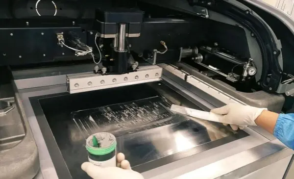
SMT Surface Mount Process
SMT Advantages
SMT has many advantages over older through-hole parts.
Smaller components. By 2012, common small sizes reached 0.4 × 0.2 mm (01005). The trend goes toward even smaller parts.
Higher component density. More parts can fit on a given area and each part can have more connections.
Higher interconnect density. SMT supports more connections per area than through-hole.
Lower cost and faster ramp to production. SMT lines can be fast and cost effective.
Fewer holes in board design and manufacturing. Fewer drilled holes reduce PCB cost and complexity.
Faster placement process. SMT placement is automated and fast.
Self-alignment of parts. Surface tension during reflow can correct small placement shifts.
Parts can be placed on both top and bottom of the board. This increases usable area.
Lower parasitic resistance and inductance. This lowers RF signal issues.
Better mechanical performance under vibration and drop. SMT often handles shock better than large through-hole parts.
Many SMT parts are cheaper than their through-hole counterparts.
Improved EMC performance. Smaller loop areas lower electromagnetic emission.
SMT Disadvantages
SMT also has some downsides.
Smaller size and fine pitch make manual repair harder. Skilled operators and expensive rework tools are needed.
SMD parts are not plug-and-play for breadboards. For quick test fixtures, you must use a custom PCB or solder SMDs onto adapter boards.
Solder joints may degrade under thermal cycling. Some solder joint failures occur from repeated temperature changes.
Finer pitch and smaller joints demand higher process precision. The SMT process must control placement and soldering tightly.
SMT is not suited for large, high-power, high-voltage parts. For example, big transformers in power supplies often still use through-hole. Many boards use a mixed approach: SMT for most parts and through-hole for large power elements.
SMT can be a poor fit where mechanical stress is frequent. Connectors that see frequent insertion and removal may stress solder joints. In those cases, through-hole or reinforced mounting is common.
PHILIFAST SMT Capabilities
Below are the SMT capabilities that PHILIFAST lists:
Maximum board size for SMT: 310 mm × 410 mm.
Maximum board thickness: 3.0 mm.
Minimum board thickness: 0.5 mm.
Smallest chip-type parts supported: 0201 package or parts larger than 0.6 mm × 0.3 mm.
Maximum part weight for placement: 150 g.
Maximum part height: 25 mm.
Maximum part footprint: 150 mm × 150 mm.
Minimum pitch for leaded parts: 0.3 mm.
Minimum BGA pitch supported: 0.3 mm.
Minimum BGA ball diameter supported: 0.3 mm.
Maximum placement accuracy for a 100 QFP: 25 μm @ IPC standard.
Why Choose PHILIFAST for SMT Assembly
Strength and capacity.
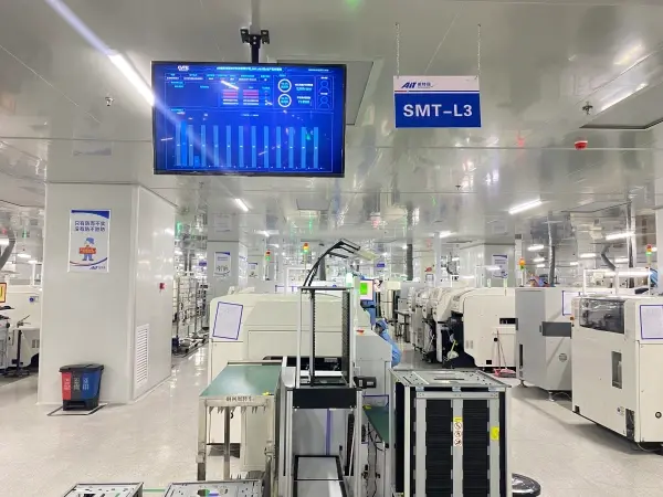
▪ SMT workshop: PHILIFAST has imported pick-and-place machines and multiple optical inspection devices. They report daily output at the scale of millions of placements. Every process stage has QC staff to monitor quality. They emphasize rich experience in SMT and soldering and stable lead times.
▪ They say they have served thousands of electronics companies. Their work includes automotive and industrial control boards. Their products often ship to Europe and North America, and customers give positive feedback about quality.
▪ On-time delivery: after receiving complete boards and parts, typical delivery is 3–5 days. For small urgent runs, same-day shipping can be arranged.Strong repair and after-sales support.
▪ PHILIFAST claims experienced repair engineers who can fix many soldering-related defects and ensure board connectivity.
▪ They offer 24-hour customer service to respond quickly to order issues.
Sammenfatning
SMT plays a central role in modern electronics manufacturing. The move from through-hole to surface mount changed many aspects of design, passive and active device choice, and manufacturing strategy. Advanced packaging methods like WLP, 3DP, and SiP push the limits of what a package can do. Each method has trade-offs in size, performance, cost, and process complexity. SMT makes assembly faster, denser, and often cheaper. But SMT also raises demands on process control and repair skill. PCBA adds value by combining assembly with sourcing and testing for a one-stop solution.
If you need SMT assembly, remember to match the package and process choices to function, heat, mechanical stress, and budget. For small and mid-volume production, suppliers who offer strong QC, flexible lead time, and reliable repair services can save time and cost. For next steps, designers should plan pad sizes, stencil openings, placement tolerances, and reflow profiles carefully. Good collaboration between PCB designers, component engineers, and the contract manufacturer ensures better first-pass yield and faster time to market.