

















PCB pads lift when a copper land separates from, or is pulled away from, the laminate surface. Common contributors include excessive or repeated heating, mechanical force, weak copper-to-laminate adhesion, unsuitable land geometry, and interactions between those factors. A lifted pad can create an open or intermittent connection and may reduce mechanical and electrical reliability, so it is a structural PCB defect rather than a cosmetic soldering issue.
This guide explains why pads lift, how to distinguish pad lifting from delamination or trace damage, how to prevent it during PCB manufacturing and assembly, and how to decide whether a damaged board can be repaired or should be rejected.
What is PCB pad lifting?
A PCB pad, also called a land, is a conductive copper area used to solder a component lead or attach a surface-mount device. It may also form the annular ring around a via. Pad lifting occurs when part or all of that copper area separates from the laminate and rises, wrinkles, cracks, or moves under light pressure. The solder joint may still look intact while the copper-to-board bond underneath has failed.
Pad lifting is different from several related failures:
- Solder-joint failure: the solder interface cracks or separates from the component lead or pad while the copper remains bonded to the board.
- Trace lifting: a routed copper conductor separates from the laminate, typically after heat or mechanical force is applied to the trace.
- Delamination: separation within the dielectric or along an internal board interface. It can cause blistering or localized swelling, and a pad may lift as a secondary effect.
- Copper peeling: a wider copper-to-laminate adhesion failure that can affect pads, traces, or larger copper areas.
The distinction matters because a solder touch-up cannot restore a pad that has lost its mechanical bond to the laminate.
Why do PCB pads lift?
1. Excessive heat during soldering or rework
Temperature changes produce different expansion responses in copper, solder, and the laminate. At elevated, material-dependent temperatures, the resin system can lose stiffness. Excessive dwell, uneven heating, or repeated cycles can then increase interfacial shear stress until the component lead or solder mass pulls the copper upward.
Risk increases when an operator repeatedly applies an iron tip to the same joint, uses uncontrolled hot air, or adds heat while mechanically moving the component. A lead-free reflow or rework process must be qualified for the solder alloy and paste, board, components, and product requirements; a guessed temperature does not define a safe process.
Use a verified SMT reflow soldering process and qualified hand-soldering work instructions. Set and record rework limits when the quality plan, customer requirement, or engineering review calls for them rather than allowing unlimited heating.
2. Mechanical force during component removal
Mechanical damage often occurs when force is applied while a relevant solder joint has not fully released. Pulling a connector, twisting a resistor, prying an IC, or levering a lead against the board transfers stress directly into the pad. Through-hole leads can act as mechanical levers, and surface-mount pads can lift when a part is dragged sideways during rework.
The same problem can occur during probing, depanelization, fixture loading, connector insertion, or removal of cured adhesive. A tool may leave no obvious scratch but still flex the copper-land interface.
Den PCBA manual soldering best practices provide process background. In an approved removal process, support the board and remove the part only after the solder has released; do not use a component body or lead as a pry point.
3. Weak copper-to-laminate adhesion
The copper foil is bonded to the dielectric through a manufactured interface. Foil treatment, resin chemistry, laminate construction, lamination conditions, surface cleanliness, and material selection can all affect adhesion. If the interface is contaminated, incompletely cured, damaged during fabrication, or poorly matched to the assembly’s thermal history, a pad may separate more easily during assembly or service.
This can be a bare-board manufacturing issue, not solely an operator issue. For critical or controlled programs, request the applicable material designation, fabrication drawing, and supplier quality records. Philifast’s guides to IPC-4101 PCB materials og FR-4 material selection explain why laminate choice and material controls matter.
4. Pad geometry and layout that concentrate stress
Small pads, narrow pad-to-trace transitions, unsupported landing areas, and layouts that transmit force through the land can concentrate stress at one edge. The peel path depends on the complete copper layout and rework process, not on trace width alone. Mechanically loaded connectors, large thermal lands, and components close to a board edge require particular attention.
During design review, check package-appropriate land patterns, annular rings, pad-to-trace transitions, solder-mask openings, component clearances, and keep-outs around mounting holes. Provide mechanical support where the assembly will see vibration or insertion force; do not rely on a soldered land alone to resist repeated connector loading. The DFT, DFM, and DFA design guide og PCB design workflow provide useful review checkpoints.
5. Thermal expansion, board flex, and material mismatch
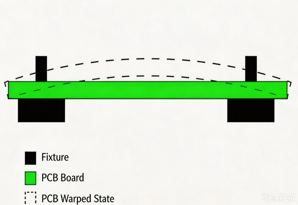
Copper and laminate do not expand identically with temperature. Through repeated heating and cooling, the interface experiences thermal stress and shear stress. Board flexing during depanelization, test, assembly, or use can add mechanical stress to the same area. The risk is higher for thin boards, large copper structures, high-temperature applications, and designs with significant differences in material properties.
CTE is only one part of the analysis. Board thickness, copper distribution, support tooling, resin system, glass-transition behavior, and local land geometry also influence the result. Tg describes a change in resin behavior and is material data to consider with the laminate supplier’s thermal limits; it is not a universal pass/fail temperature. See how CTE affects PCB reliability and design when evaluating thermal cycling or mechanically demanding applications.
6. Moisture, delamination, and rework history
Moisture absorbed by the board or component can contribute to cracking, blistering, or delamination during rapid heating, depending on material condition and the heating process. A previously reworked area may already have weakened copper adhesion even if the pad still looks flat. A later repair can then lift the pad with less force than the original assembly process.
Control storage, baking, handling, and rework records according to the board and component suppliers’ instructions. For moisture-sensitive surface-mount devices, use a handling plan consistent with IPC/JEDEC J-STD-033; bare-board storage and baking conditions remain material- and supplier-specific. A lifted pad near a blister, white halo, resin crack, or other delamination sign warrants investigation as a broader material or thermal event rather than repair in isolation.
Philifast — PCB Manufacturing & Assembly Services
We help you prevent pad lifting through DFM review, qualified soldering processes, and strict quality control.
Does rework cause lifted PCB pads?
Yes. Rework is a common cause of PCB rework damage when heat, dwell time, tool pressure, and component movement are not controlled. The risk is not determined by temperature alone: contact area, thermal recovery, board thickness, copper mass, solder alloy, pad geometry, and the number of previous cycles all matter. A process that removes one small passive safely may damage a fine-pitch IC or connector.
Before rework, identify the approved method, maximum allowed attempts if specified, board support, and inspection requirements. Use thermally controlled tools, suitable nozzles, preheating when qualified, and localized shielding where needed. After rework, inspect the pad and nearby solder mask under magnification and perform the electrical test required by the product risk.
Warning signs and detection methods
Early detection can help contain a local pad defect before it becomes a trace or laminate repair. Look for:
- a pad edge that is visibly raised, curled, or wrinkled;
- unintended movement of a pad or component lead observed during controlled inspection;
- a solder fillet that moves while the copper underneath stays displaced;
- solder-mask cracking, discoloration, blistering, or a white halo around the land;
- intermittent continuity, changing resistance, or a functional failure after light board flex;
- a pad that appears intact in top view but shows separation on cross-section or mechanical examination.
Select inspection according to the product risk and quality plan. Visual inspection and microscopy can reveal surface lifting; continuity or in-circuit testing can show an electrical consequence, but a passing test does not prove adequate mechanical adhesion. Cross-section analysis may be appropriate for root-cause confirmation, suspected delamination, or a disputed failure. The PCBA testing process guide explains how electrical and physical inspection complement one another.
What are the risks of a lifted pad?
The primary risk is an open circuit or intermittent connection. A damaged pad can also reduce solderable area, expose laminate, concentrate stress in a nearby trace, or make a later repair more difficult. On power, high-current, high-frequency, safety-related, or mechanically loaded circuits, the consequence may be greater than the visible size of the defect suggests.
Reliability depends on the pad’s electrical role, remaining copper area, mechanical loading, environmental exposure, and the quality of any repair. Do not approve a lifted land solely because the board passes a short functional test. Define acceptance and repair criteria in the drawing or quality plan before production.
How can PCB pad lifting be prevented?
Design controls
- Use a package-appropriate land pattern and verify pad-to-trace transitions.
- Ensure annular rings and land features meet the applicable design and fabrication requirements; review routing and mechanical support for loaded connections.
- Keep high-force connectors, mounting holes, and depanelization features away from vulnerable pads.
- Consider board thickness, laminate system, Tg and other supplier thermal data, copper distribution, and thermal cycling during stack-up and DFM review.
- Add test points and access that reduce the need to probe component pads.
Manufacturing controls
- Specify PCB materials, stack-up, and fabrication requirements appropriate to the product.
- Use incoming inspection and supplier quality evidence appropriate to the program to review solder-mask damage, warpage, delamination indicators, and possible adhesion concerns.
- Use panel support and depanelization methods that do not flex the board excessively.
- Profile reflow and selective or wave soldering on representative assemblies.
- Track nonconformances by lot, panel position, material batch, and process revision.
Assembly and rework controls
- Use soldering profiles and hand-soldering instructions qualified for the board, components, and solder alloy.
- Preheat and support the board when the qualified process requires it.
- Avoid twisting or pulling components while solder remains solid.
- Limit rework cycles and use a defined escalation path for damaged pads.
- Inspect repaired areas with magnification and perform the electrical or functional checks required by the quality plan.
Philifast — PCB Pad Lifting Prevention
Our DFM and process control expertise helps you avoid pad lifting in high-reliability products.
Can a lifted PCB pad be repaired?
Sometimes, but the correct disposition depends on the damage, circuit function, product specification, and customer workmanship requirements. Under a qualified repair procedure, a repair may use a replacement land or an engineered jumper to restore the net. The repair must restore the required electrical connection and mechanical support for the product’s use conditions.
Do not simply press the pad flat and add solder. That can hide a weak interface and leave an intermittent fault. A repair decision should consider whether the pad is connected to a trace or via, whether the laminate is damaged, whether adjacent conductors are exposed, the required current and voltage, thermal cycling, vibration, creepage and clearance, and whether the repair is allowed by the customer’s workmanship standard.
For production, use a documented repair procedure, trained personnel, approved materials, inspection evidence, and traceability. Where invoked, IPC-7711/7721 provides rework, modification, and repair guidance; it does not override the product specification or customer requirements. For safety-critical or high-reliability assemblies, repair may be restricted or prohibited by the contract or quality plan. An engineering prototype can sometimes be repaired for evaluation, but that does not qualify the method for production or shipment.
A practical troubleshooting workflow
When a pad lifts, contain the affected lot or board before rework continues. Record the reference designator, board side, panel position, component type, rework station, tool, solder alloy, number of thermal cycles, and operator or program revision. Then inspect the area under magnification and compare it with an unaffected pad.
Use the pattern of failures to guide the investigation:
- One pad on one board: suspect local handling, rework force, or an isolated board defect.
- The same footprint across a panel: review the land pattern, stencil or soldering setup, panel support, and board fabrication.
- Pads near a connector or edge: investigate mechanical loading, depanelization, and fixture contact.
- Pads lifted after several repairs: review thermal history, dwell time, and the rework limit.
- Pads with blisters or widespread copper separation: investigate laminate, moisture, and delamination rather than treating it as a local solder issue.
Confirm the suspected cause with a controlled sample or cross-section, then update the process control plan. Sorting and repeated manual touch-up are not substitutes for correcting the cause.
OFTE STILLEDE SPØRGSMÅL
Why do PCB pads lift during soldering?
Pads can lift when elevated heat reduces the laminate’s mechanical margin and soldering force pulls the component or land upward. Repeated heating, excessive dwell, poor board support, weak or contaminated adhesion interfaces, and stress-concentrating geometry can all contribute.
Does a lifted pad always mean the PCB is unusable?
No. A board may be repairable when the net, surrounding laminate, product specification, and customer requirements permit an approved repair. A passing continuity test alone is not enough; the repair must be inspected and qualified for the product’s electrical, thermal, and mechanical conditions.
Can soldering temperature alone cause pad lifting?
Temperature set point is only one factor. Time at temperature, heating rate, tool pressure, board support, copper mass, solder alloy, land geometry, and previous rework cycles also affect stress on the land. Use a qualified profile and work instructions rather than a single temperature number.
What is the difference between pad lifting and delamination?
Pad lifting is separation of a copper land from the board surface. Delamination is separation within the laminate or between board layers. They can occur together, but delamination usually calls for a broader material and thermal investigation.
How can a manufacturer prevent copper pad lifting?
The manufacturer should control laminate and copper materials, verify fabrication quality, review land and trace geometry, support the panel during assembly, qualify soldering processes, control rework, and record pad-related nonconformances by lot and process revision.
Should a lifted pad be repaired or rejected?
Use the product drawing, customer workmanship standard, circuit criticality, and documented repair procedure. Reject or replace the board when the laminate or adjacent conductors are damaged, the remaining connection is not mechanically sound, the contract prohibits repair, or the repair cannot be validated for the product environment.
Philifast — Your PCB Manufacturing Partner
From design to assembly, we deliver reliable boards with controlled pad adhesion and quality.

