


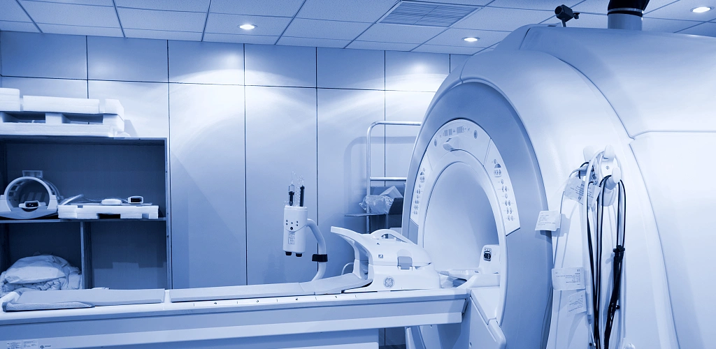
Medical PCBs are the nervous system of modern healthcare. They live inside pacemakers, imaging machines, patient monitors, and robotic surgery tools. A single board failure can risk a life. So every medical PCB demands zero-defect manufacturing, full traceability, and strict adherence to standards our factory has mastered over 15 years.
We do not just talk about reliability. We build boards that meet IPC‑6012 Class 3, support IEC 60601‑1 clearance rules, and come with an ISO 13485‑audited quality system. In this article, you will learn how to design, specify, and source a medical PCB that passes regulatory scrutiny — and how to avoid the hidden pitfalls that generic PCB shops never mention. We will also break down real medical PCB costs, lead times for Class 3 quick‑turn, and the DFM rules that prevent field failures.
Medical PCB Applications and Types
Medical devices push PCB technology to its limits. A hearing aid needs a flexible circuit so thin it can fold into an ear canal. An MRI coil requires dielectric materials with zero magnetic signature. A CT scanner processor board may carry hundreds of high‑speed signals on 20+ layers. Below are the most common PCB types you will specify.
- High‑Density Interconnect (HDI) Medical PCBs
When space is the scarcest resource, HDI packs more connections into less area. We build HDI boards with laser‑drilled microvias down to 75 µm, multiple build‑up layers, and via‑in‑pad structures. Use HDI for handheld ultrasound probes, capsule endoscopes, or implanted neurostimulators where every millimeter matters. - Flex and Rigid‑Flex Medical PCBs
Devices that bend, twist, or must survive millions of dynamic cycles need flex circuits. A wearable glucose monitor contains a polyimide flex that wraps around a wrist while routing 0.10 mm traces. Rigid‑flex eliminates connectors — a major source of failure in body‑worn electronics. Our factory laminates polyimide flex layers with FR‑4 rigid sections, then fills transition vias with non‑conductive epoxy for structural integrity. - Rigid PCBs for Hospital Equipment
Large‑format rigid boards for X‑ray detectors, ventilators, and lab analyzers often run on standard FR‑4 with high copper weight (2 oz or 3 oz) for thermal management. We can produce up to 32‑layer rigid medical PCBs with controlled impedance, blind/buried vias, and ENIG surface finish.
No matter the type, the board must match the electrical, thermal, and mechanical demands of the application. Next, we detail the mandatory compliance framework.
Key Compliances for Medical PCBs
A PCB is just a component of a medical device. But the fabrication process itself must demonstrate control and repeatability. These are the standards our factory lives by.
ISO 13485:2016 Quality Management
ISO 13485 is not a PCB standard; it is a quality‑system certificate specific to medical device components. Our facility holds ISO 13485 certification with a scope that explicitly covers PCB fabrication. An annual surveillance audit verifies document control, traceability of raw materials, and process validation (IQ/OQ/PQ). For you, that means every production lot comes with a Device History Record (DHR) — a complete paper trail from laminate batch to final electrical test.
IPC‑6012 Class 3 and IPC‑A‑600 Inspection
Class 3 is the highest reliability grade for PCBs. It demands:
- Minimum annular ring of 0.125 mm on drilled holes.
- No lifted lands, nicks deeper than 20% of conductor width, or plating voids.
- 100% micro‑section analysis per lot — we cut two cross‑sections per panel to measure copper thickness in holes (minimum 20 µm) and check for inner‑layer separation.
We inspect finished boards to IPC‑A‑600 Class 3 acceptance criteria using 2D/3D AOI with comparison to the original Gerber data. Any board with a mismatch goes to manual review. We also perform 4‑wire Kelvin netlist testing to catch opens and shorts that visual inspection misses.
IEC 60601‑1 and Creepage/Clearance
The medical safety standard IEC 60601‑1 defines minimum creepage and clearance distances to prevent electric shock. A PCB shop cannot “certify” a bare board to IEC 60601‑1; that is your device‑level responsibility. But we can build to any creepage value you specify — and we verify it with automated optical measurement reports. For high‑voltage isolation (above 250 V), we also enforce design rules that prevent conductive anodic filament (CAF) formation, which we cover in the DFM section.
FDA Registration
Our factory is FDA‑registered as a contract manufacturer. That does not replace your device listing, but it means we operate under a quality system recognized by the FDA. If you need a supplier who can provide full traceability for a 510(k) or PMA submission, we meet that requirement.
Choosing Materials for Medical PCBs
Material selection drives both performance and compliance. A poorly chosen laminate can lead to CAF growth between biased traces, delamination during autoclave sterilization, or signal integrity loss in high‑speed imaging.
Below is a comparison of the materials we use most often for medical applications.
| Material | Tg (°C) | CTI (V) | Dk @1 GHz | Water Absorption (%) | Z‑axis CTE (ppm/°C) | Typical Medical Use |
|---|---|---|---|---|---|---|
| Standard FR‑4 (Tg 150) | 150 | 175–250 | 4.2–4.5 | 0.15 | 50–70 | Non‑critical monitoring, lab equipment |
| High‑Tg FR‑4 (Tg 170) | 170 | 200–300 | 4.0–4.3 | 0.12 | 35–45 | High‑layer‑count imaging, ventilators |
| Isola 370HR | 180 | 400+ | 3.9 | 0.10 | 35 | High‑voltage isolation, defibrillator circuits |
| Polyimide (flex) | 250 | 300–600* | 3.4–3.6 | 1.0–2.0** | 40–60 (film) | Wearables, flexible probes, dynamic flexing |
| Rogers 4350B | >280 | 165 | 3.48 | 0.06 | 32 (X/Y) | RF coils for MRI, wireless patient telemetry |
| Liquid Crystal Polymer (LCP) | 280 | >500 | 2.9–3.2 | <0.02 | 17–30 | Implantable flex with long‑term body‑fluid resistance |
CTI of polyimide depends on the specific laminate grade; consult the supplier data sheet.
Polyimide absorbs moisture; for implantables that must remain dry, LCP is superior.
For most Class 3 designs, we recommend high‑Tg FR-4 like Isola 370HR because its CTI above 400 V allows smaller creepage distances. When the device contacts the patient directly, we often switch to Rogers or LCP to avoid CAF under humid or ion‑rich conditions. Our engineering team can help you pick the right material for your stackup and reliability budget.
DFM Checklist for High‑Reliability Medical PCBs
Design‑for‑manufacturability (DFM) prevents failures before the first board is built. These rules come from failure analysis of real medical devices.
- Creepage and Solder Mask Dam Width.
Meeting bare‑copper creepage per IEC 60601‑1 is not enough. In a humid environment, moisture can form a conductive path across the solder mask surface. We enforce a minimum mask dam of 0.20 mm between high‑voltage traces on the same layer. This barrier blocks ion migration and reduces the risk of CAF. - Inner‑Layer Pad Anti‑Pad Clearance for Flex.
When laser drilling microvias through a polyimide flex layer, the drill can drag copper slivers from the inner pad if the anti‑pad gap is too small. Set the clearance to at least 0.30 mm to avoid slivering and subsequent short circuits. - Via‑in‑Pad Restrictions for Dynamic Flex.
Avoid placing via‑in‑pad on a flex circuit that will bend repeatedly. The stress concentration around the via can crack the barrel. If you must use via‑in‑pad for density, specify non‑conductive epoxy fill and cap with ENIG to create a flat surface. - Copper Weight for Heat Spreading.
In an active implant like a neurostimulator, the PCB must dissipate heat from a small area without fans or vents. Increase the copper weight on inner power planes to 2 oz or more. This thermal mass spreads heat laterally and reduces hot‑spot temperature. - Controlled Impedance with Tight Tolerance.
Many medical imaging and RF ablation systems require ±7% or ±5% impedance control on differential pairs. Our factory calculates the stackup using the actual Dk value of the laminate (not just the supplier’s nominal) and adjusts line width accordingly. We verify every impedance coupon with TDR and include the test report in the DHR.
Putting these rules into your design reduces NRE cycles and ensures the PCB passes IPC Class 3 inspection on the first build.
Medical PCB Cost Breakdown: From Prototype to Production
Medical PCB pricing is not a mystery. It follows a clear formula, and understanding it helps you budget and negotiate.
Four factors dominate the medical PCB price:
- IPC Class.
Class 3 adds roughly 18–22% to the fabrication cost versus Class 2. The increase covers extra inspection steps (100% AOI, mandatory micro‑sectioning, tighter drill registration) and the higher scrap rate from rejecting boards that would pass Class 2 criteria. - Layer Count and Thickness.
A 4‑layer Class 3 board with a 1.6 mm overall thickness costs less than an 8‑layer board of the same size. Each additional layer pair adds lamination, drilling, and plating cycles. - Surface Finish.
ENIG (electroless nickel immersion gold) is the most common medical finish because it provides a flat, solderable surface with good shelf life. Immersion silver offers better high‑frequency performance but must be soldered within a shorter window. ENIG typically adds 12–15% to the board cost versus HASL (which we do not use for medical). For implantable contacts, hard gold plating over nickel is required to withstand body‑fluid corrosion — that process adds a premium. - Quantity and Panel Utilization.
Prototype quantities (10–50 pieces) have high NRE charges and low panel efficiency. At 500 units, we can gang multiple boards on a panel to amortize tooling costs. Our factory does not have a fixed MOQ for medical PCBs; we produce as few as 5 panels for prototype runs. However, lower quantities drive up the per‑unit cost.
Example cost range (4‑layer, 100×150 mm, ENIG finish, Class 3, FR‑4 Tg 170, standard lead time):
- 10 pcs: $45–60/unit
- 500 pcs: $12–18/unit
- 2,000 pcs: $7–10/unit
These are estimates. We provide a fixed‑price quote after reviewing your Gerber files and stackup requirements.
Medical PCB Lead Times – What to Expect
“Quick‑turn Class 3” does not mean 24 hours. A true Class 3 medical PCB requires time for multiple quality gates.
Our standard lead time for a 4‑layer Class 3 board is 8–10 working days. An 8‑layer board might take 12–15 days. The extra time is needed for:
- Two micro‑section coupons per fabrication panel (cross‑sectioning, mounting, polishing, and measurement).
- 100% electrical test using flying probe or fixture, depending on quantity.
- Final AOI and visual inspection to IPC‑A‑600 Class 3.
We do offer expedited 5‑day service on 4‑layer boards if you accept a risk waiver to reduce micro‑section sampling to one coupon. We do not recommend this for implantable or life‑sustaining devices, because a latent plating void might only appear after thermal cycling. For critical projects, always choose the standard lead time with full lot verification.
Our factory communicates the delivery schedule at the quote stage, and we ship on time. If your project needs a faster spin, ask our engineers about available capacity — we can sometimes fit a rush order without compromising test coverage.
How to Audit a Medical PCB Supplier
A valid ISO 13485 certificate is just the starting point. When you evaluate a PCB partner, dig deeper.
- Scope of Certification.
Confirm the ISO 13485 certificate explicitly covers PCB fabrication, not just assembly or contract manufacturing. Ask for the latest audit report summary to see any non‑conformities and their resolution. - FDA Registration Status.
Being FDA‑registered means the facility is listed as a contract manufacturer and follows Good Manufacturing Practices (GMP). Request the FDA establishment registration number and verify it on the FDA website. This registration supports your own device submission because it demonstrates a controlled supply chain. - Process Validation Records.
Critical processes like ENIG plating, microvia formation, and lamination must have IQ/OQ/PQ documentation. Ask to see the protocol for plating thickness control, including SPC charts. A supplier that cannot show validated processes will not pass a rigorous regulatory audit. - In‑House Test Capabilities.
The best medical PCB suppliers perform all testing internally — no subcontracting. We have flying probe testers, TDR for impedance, micro‑section lab, and ionic contamination testers in‑house. This single‑site control eliminates communication gaps and keeps your data secure. - Traceability.
For every order, you should receive a DHR containing the certificate of conformance, material lot numbers, first‑article inspection report, copper plating thickness data, AOI reports, electrical test results, and ionic cleanliness report. If the supplier hesitates to provide all of these, consider it a red flag.
We encourage on‑site audits. You can walk through our class‑10,000 cleanroom and see exactly how we build your boards. That transparency is what full medical PCB supplier qualification demands.
Häufig gestellte Fragen
What is the minimum order quantity for medical PCBs?
We do not enforce a hard MOQ. We build as few as 5 prototype panels for medical PCB validation. However, single‑piece or very small runs carry a higher unit cost due to NRE and panel setup charges.
How do you ensure impedance control on medical PCBs?
We calculate the stackup using the laminate’s measured dielectric constant, adjust trace geometry, and place an impedance coupon on every panel. We test each coupon with a TDR and include the results in the DHR. Tolerances of ±7% are standard; ±5% is available on request.
Do you provide ENIG surface finish for medical applications?
Yes, ENIG is our default medical finish. We plate 3–5 µm of nickel and 0.05–0.10 µm of immersion gold per IPC‑4552. For implantable contacts that require repeated mating, we offer hard gold plating over nickel.
What is the difference between ISO 13485 and IPC‑6012?
ISO 13485 is a quality management standard for medical device components. IPC‑6012 is a performance specification for rigid PCBs. We hold both: our ISO 13485 system ensures process control, and our boards are built and inspected to IPC‑6012 Class 3.
How quickly can I get a Class 3 medical PCB prototype?
Our 5‑day expedited service is available for 4‑layer designs with a risk‑acknowledgement waiver on one micro‑section. For full Class 3 lot verification, standard lead time is 8–10 working days.
Do you support rigid‑flex medical PCB designs?
Absolutely. We laminate rigid FR‑4 sections to polyimide flex layers, fill transition vias with non‑conductive epoxy, and apply coverlay or liquid photo‑imageable solder mask as needed. We also build LCP‑based rigid‑flex for body‑fluid resistant implants.
Can you help with DFM for a wearable medical device?
Our engineers review every design for creepage, CAF risk, via‑in‑pad stress, and impedance. We provide a detailed DFM report with suggested changes before production starts. This service is free with every order.
What documentation comes with the shipment?
You receive a Device History Record containing certificate of conformance, material specifications, first‑article inspection report, reflow profile copy (if assembly is included), AOI/visual inspection report, electrical test report, ionic cleanliness result, and any micro‑section analysis images. This supports your regulatory file.
Get Your Medical PCBs Built with Full Traceability
A medical device is only as reliable as the PCB at its core. Do not leave that reliability to chance. We combine ISO 13485‑certified processes, IPC Class 3 manufacturing, FDA registration, and 15 years of factory‑floor experience into every board we ship. Whether you need a quick‑turn HDI prototype or a production run of rigid‑flex circuits, we offer transparent pricing, documented quality, and engineering support from design review to final delivery.
Get a Free Medical PCB DFM Review
Upload your Gerber files and BOM for a fast engineering review. Our team will provide a detailed quotation, manufacturability check, and lead time confirmation within one business day.