In PCBs, many things can cause EMI. For example: radio frequency currents, common-mode voltages, ground loops, impedance mismatch, and magnetic flux. To control EMI, we need to learn these causes step by step and see how they affect the board. We can study the math from electromagnetic theory. But that path is long and hard. For most engineers, clear and simple words are more useful. This article will cover: the “sources of electric fields” on a PCB, how to use Maxwell’s equations, and the idea of minimizing magnetic flux.
1. Sources of Electric Field
1.1 Electric Dipole Model (Time-Varying)
The source of electric fields is often modeled as a time-varying electric dipole. This is the opposite idea of a magnetic source. An electric dipole means two close, opposite point charges that change with time. The two ends of the dipole show a change in charge. This happens because current flows along the whole length of the dipole. You can model an electric source by driving an unterminated antenna with an oscillator signal. This circuit shows how an electric source works. But you can not explain it using only low-frequency circuit ideas.
Do not forget that signal propagation speed is not infinite. The speed depends on the dielectric constant of non-magnetic materials. Because speed is finite, RF current will appear in the circuit. People sometimes assume the wire has the same voltage at every point and that the circuit is always in balance at every instant. This is not true at RF.
1.2 Key Factors Affecting Electromagnetic Fields
The electromagnetic field from an electric dipole depends on four things:
- Current amplitude in the loop: The field is proportional to the current that flows in the dipole.
- Dipole polarity and the measurement antenna: The dipole’s polarity must match the antenna polarity of the measurement tool. This is like a magnetic source.
- Dipole size: The field is proportional to the length of the current element. But the line length must be only a part of a wavelength. The larger the dipole, the lower the frequency measured at the antenna. For a given size, the antenna will resonate at a certain frequency.
- Distance: Electric and magnetic fields are linked. Their strength depends on distance. In the far field, the behavior is like a loop (magnetic) source and you see an electromagnetic plane wave. Close to the point source, the field’s dependence on distance is stronger.
1.3 Near Field vs. Far Field Relationships
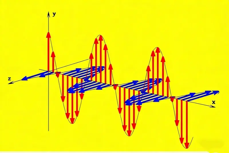
Near field and far field include both magnetic and electric parts. All waves combine electric and magnetic parts. This mix is the Poynting vector. In fact, there is no pure “electric wave” or “magnetic wave” alone. We can measure a plane wave because, for a small antenna several wavelengths away, the wavefront looks like a plane.
A small drawing can help. It would show wave impedance and distance. The labels would read: wave impedance; electric-field-dominant region with E = 1/r and H = 1/r²; plane wave with Z = 377 Ω; asymptote line; real shape; magnetic-field-dominant region; transition area; near field H = 1/r³, E = 1/r²; far field; horizontal axis 0.1, 0.5, 1.0, 5.0.
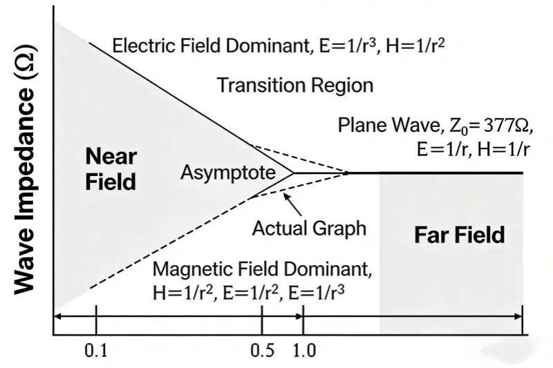
This view is the physical “profile” the antenna sees. Think of it like throwing a stone into a river and seeing ripples. The field radiates from a point source at the speed of light. The speed depends on the dielectric constant. The unit for the electric field is V/m. The unit for the magnetic field is A/m. The ratio E to H is the free-space impedance. For a plane wave in free space, wave impedance Z₀ is constant. It does not depend on distance or on the point source. A plane wave in free space carries energy in watts per square meter.
1.4 Noise Coupling and Lumped Component Models
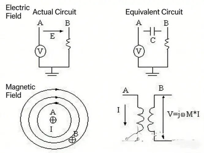
For most uses of Maxwell’s equations, we model noise coupling with equivalent lumped components. For example: a time-varying electric field between two conductors is like a capacitor. A time-varying magnetic field between the same two conductors is like mutual inductance. A figure can show these two noise coupling paths.
For such noise models to be correct, the circuit must be small compared to the signal wavelength. If that is not true, we can still use lumped component models to describe EMC. Why? Because Maxwell’s equations are hard to apply in many real cases due to complex boundaries. If the lumped model seems roughly correct, it is useful. Most discrete components usually behave reliably.
A numerical model will not always show how noise arises from system parameters. A model may be an answer, but system parameters may not be known, found, or visible. Among available models, lumped-component models are often the best practical choice.
1.5 Significance for PCB Layout
Why do we study this theory for PCB layout? The simple answer: we must know how electromagnetic fields are made. Then we can reduce RF fields on the PCB. This means we must reduce RF currents in the circuit. RF current links to the signal distribution network, bypassing and coupling. RF current finally forms harmonics and other digital signal content. Signal distribution networks must be as small as possible. That reduces the area of RF return current loops. Bypass and coupling relate to large currents and must occur through the power distribution network. By definition, the power distribution network has large RF return loop areas.
2. Applying Maxwell’s Equations
2.1 Linking Maxwell’s Equations to Ohm’s Law
We introduced Maxwell’s basic ideas above. But how do we apply this physics and calculus knowledge to EMC on a PCB? We must simplify Maxwell’s equations to use them for PCB traces. We can link Maxwell’s equations to Ohm’s law.
Ohm’s law in time domain:
V = I × R.
Ohm’s law in frequency domain:
V_rf = I_rf × Z.
Here V is voltage, I is current, R is resistance, and Z is impedance (Z = R + jX). rf means radio frequency energy. If RF current exists in a PCB trace that has a fixed impedance, an RF voltage will be created. The RF voltage is proportional to RF current. Note: in the wave model, R is replaced by Z. Z is complex. It has resistance (real) and reactance (imaginary).
2.2 Impedance Formulas for Wires/PCB Traces
There are many ways to write impedance, depending on whether we look at plane wave impedance or circuit impedance. For wires or PCB traces, we use:
Angular frequency:
ω = 2πf.
Inductive reactance:
X_L = 2πfL.
Capacitive reactance:
X_C = 1 / (2πfC).
Impedance:
Z = R + jX_L + 1/(jX_C) = R + jωL + 1/(jωC).
When a component has known resistance and inductance, for example a ferrite bead-on-lead, a resistor, a capacitor, or devices with parasitics, we must consider that impedance changes with frequency.
2.3 Current Path Selection Mechanism
Above some kHz, reactance usually becomes larger than R. But not always. Current chooses the path of least impedance. Below some kHz, resistance may be the smallest path. Above some kHz, reactance may rule. Many circuits operate above kHz, so the simple idea “current picks the path of least resistance” no longer fully explains how current flows on a transmission line.
For conductors carrying current above 10 kHz, the current will pick the path with the least impedance. If load impedance connects to a wire, cable, or trace and is larger than the parallel capacitance on the transmission path, inductance will dominate. If all connected wires have similar cross-section, the path with the smallest loop area has the smallest inductance. The smaller the loop area, the smaller the inductance. So current flows that way.
2.4 Impact of Trace Inductance on RF Energy
Every trace has a finite impedance. Trace inductance is the only reason RF energy can exist on a PCB. Long bond wires between a silicon chip and a mounting pad can also cause RF energy. Routing on a board can make high inductance, especially when traces are long. A long trace means the round-trip length is long. This causes time delay in the trace. One signal can be launched before the earlier one returns. In the frequency domain, a trace becomes “long” when its total length is larger than about λ/10 at a frequency present in the trace.
In short: an RF voltage across an impedance makes RF current. This RF current can radiate energy into free space and break EMC limits. These examples link Maxwell’s equations to PCB routing with simple math.
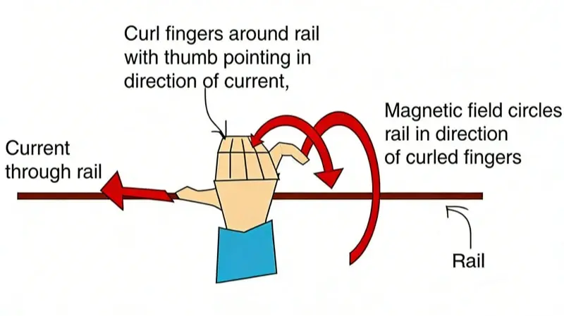
2.5 Right-Hand Rule for Magnetic Flux Direction
Maxwell says moving charge on a trace makes current. Current makes a magnetic field. These magnetic lines of flux follow the trace. Use the right-hand rule to find flux direction. Point your thumb in the current direction. Your curled fingers show the magnetic field around the trace. A time-varying magnetic field makes a perpendicular electric field. RF radiation is the mix of this magnetic and electric field. The fields can leave the PCB by radiation or by conduction along connected cables.
Note that the magnetic field runs around a closed loop boundary. On a PCB, the source drives RF current from source to load through a trace. The RF current must return to the source (Ampere’s law). This makes an RF current loop. The loop need not be circular, but often is spiral. Because the return path creates a closed loop, it makes a magnetic field. The magnetic field creates a radiated electric field. In the near field, magnetic parts may dominate. But in the far field, the ratio E/H (wave impedance) is about 120π Ω, or 377 Ω. That value does not depend on the source. So in the far field, one can use a loop antenna and a sensitive receiver to measure the magnetic part. The received current is E/(120π) in A/m if E is in V/m. You can also measure the electric part with proper tools in the near field.
2.6 Importance of Closed-Loop Circuits
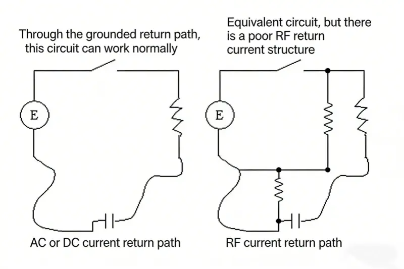
Another simple view of RF on PCBs comes from typical circuits shown in figures. Use time domain and frequency domain analysis. Kirchhoff and Ampere laws say a closed loop must exist for a circuit to work. Kirchhoff’s voltage law says the sum of voltage around any closed path is zero. Ampere’s law says a current makes magnetic induction at a point, based on the current and geometry.
If a closed loop did not exist, a signal could not travel from the source to the load on a transmission line. When a switch closes, the circuit forms and AC or DC current flows. In the frequency domain, this current is RF energy. There is not a separate kind of current in time or frequency domain. One current exists and we can see it in either domain. The RF return path must exist from load to source, otherwise the circuit cannot work. Therefore PCB structure must obey Maxwell, Kirchhoff, and Ampere.
All these laws say: to run a circuit as expected, a closed loop network must exist. A figure would show such a typical circuit. When a trace goes from source to load, its return current path must exist. That is Kirchhoff and Ampere.

A second figure would show a switch and a driver E in series. When the switch is closed, the circuit works. If open, it does not. In time domain, the desired signal goes from source to load. The signal must have a return path, usually through a 0V ground reference. RF currents flow from source to load and return through the path with the least impedance. Often this is through a ground trace or plane, a mirror plane. Use Ampere’s law to explain RF current.
3. Flux Minimization (Magnetic Flux Minimization)
3.1 Mechanism of Magnetic Flux Generation
Before we study “how EMI appears in a PCB,” we must learn how magnetic lines form on transmission lines. Magnetic flux is a core idea. Flux forms when current flows through a fixed or varying impedance. Impedance exists in traces, component leads, vias, and so on. If flux exists on the PCB, Maxwell says RF energy paths also exist. Those paths can radiate into free space or conduct away through cables.
3.2 Principle of Flux Cancellation
To remove RF current on the PCB, we use “flux cancellation” or “flux minimization.” Magnetic lines run in one direction around the trace. If we make the RF return path parallel and close to the source trace, then the return path’s field runs opposite to the source field. When fields run in opposite directions, they cancel. If unwanted flux between source and return is canceled or kept small, radiation or conducted RF current will not exist, except at very small trace edges. The concept of canceling flux is simple. But in design, watch for traps and small mistakes. A small error can cause many extra problems that make debugging hard.
The easiest flux cancellation method is to use an image plane (mirror plane). No matter how well you route, electric and magnetic fields will always exist. But if you cancel magnetic lines, EMI is gone. It is that simple.
3.3 Flux Minimization Tips in PCB Layout
How to cancel flux in PCB layout? There are many tips. Not all directly cancel flux. Some common ones:
- Use multi-layer boards with correct stackup assignment and impedance control.
- Route clock traces near the return ground plane (in multilayer PCBs). For single- or double-sided boards, use ground traces or guard traces near clock traces.
- Capture magnetic flux from inside plastic packages into the 0V reference to lower component radiation.
- Choose logic parts carefully to reduce the RF spectrum the parts radiate. Use devices with slower edge rates when possible.
- Reduce RF drive voltage from clock drivers (TTL/CMOS) to lower RF current on traces.
- Lower ground noise voltage that exists between power and ground planes.
- When many device pins switch at once to drive a large capacitive load, provide enough decoupling for the part.
- Properly terminate clock and signal traces to avoid ringing, overshoot, and undershoot.
- Use data-line filters and common-mode chokes on networks that need them.
- For external I/O cables, use bypass capacitors correctly (not as decoupling).
- For components that radiate a lot of common-mode RF energy, give them a grounded heat sink.
3.4 Other Causes of EMI in PCBs
Looking at the list shows magnetic flux is only one part of EMI on PCBs. Other causes include:
- Common-mode and differential-mode currents between circuit and I/O cables.
- Ground loops that generate magnetic field structures.
- Radiating components.
- Impedance mismatch.
Note: most EMI radiation comes from common-mode voltages. On a board or circuit, these common-mode levels can be turned into small fields.
Schlussfolgerung
To remove EMI on PCBs, start with reducing magnetic flux. Saying it is easy, but doing it is harder. RF energy is invisible and hard to find. By locating where RF current flows and which way it flows, and by using the tips above and the rules from Maxwell, Kirchhoff, and Ampere, you can narrow the suspect area. Then find the true EMI source and remove it.