En el diseño de placas de circuito impreso debemos prestar atención a las vibraciones. Debemos prever la fatiga por vibraciones. Si no lo hacemos, la placa no durará mucho. Muchas placas están quietas y no se mueven mucho. Otras placas trabajan en lugares con mucho movimiento. Estos dispositivos pueden ser desde pequeños juguetes hasta complejas naves espaciales. Algunas placas no se mueven, pero siguen sometidas a tensiones de fabricación, cambios térmicos o golpes fuertes de los usuarios. Para hacer frente a esto, Diseñadores de PCB necesitan conocer los aspectos básicos de la fatiga por vibraciones en sus diseños y cómo reducir sus efectos. He aquí algunas ideas que ayudan.
Estrés ambiental y fatiga por vibraciones
Hasta 20% de los fallos de las placas de circuito impreso se deben a vibraciones y golpes. Estas cifras fueron citadas por primera vez por la Fuerza Aérea, pero muchas otras industrias informan de tasas similares. Esto demuestra lo importante que es diseñar placas de circuito impreso resistentes a la fatiga por vibraciones aleatorias. Esto es más importante en las placas utilizadas en entornos propensos a las vibraciones, como el aeroespacial.
Materiales del núcleo del tablero (por ejemplo FR-4) soportan bastante bien las vibraciones y los golpes. Pero los componentes electrónicos soldados a la placa no. Las vibraciones hacen que la placa se doble. Los cables de los componentes pueden romperse al doblarse y estirarse. La soldadura también es vulnerable a las vibraciones. Puede agrietarse y romper el enlace eléctrico entre un cable y la placa. Incluso una pequeña vibración prolongada puede fatigar los cables de los componentes y las juntas de soldadura. Sin unas buenas prácticas de diseño de PCB, las juntas de soldadura pueden agrietarse debido a la fatiga por vibraciones.
Las tensiones de fabricación pueden provocar fatiga por vibraciones
Otro factor que conduce al fallo por fatiga por vibración es la tensión del Fabricación de PCB proceso. Los cables de los componentes y las juntas de soldadura son vulnerables a los choques térmicos. Unas buenas prácticas de DFM (diseño para la fabricación) son fundamentales para controlar estos efectos. Un ejemplo es el diseño de almohadillas en la placa de circuito impreso para que los cables de los componentes puedan soldarse correctamente.
Unas zapatas mal diseñadas pueden impedir que la soldadura rellene correctamente los conductores de montaje superficial. La soldadura puede desprenderse de una almohadilla de orificio pasante. Estos problemas pueden provocar una mala conexión de la soldadura. Por ejemplo, en una almohadilla térmica grande, la pérdida de soldadura de una vía descubierta puede impedir que la clavija de masa de un dispositivo tenga una buena conexión de soldadura. Esa pieza puede pasar la fabricación y la prueba. Pero las vibraciones pueden desgastar una fina unión soldada hasta que falle de forma intermitente o por completo sobre el terreno.
¿Qué puede hacer para prevenir la fatiga por vibraciones?
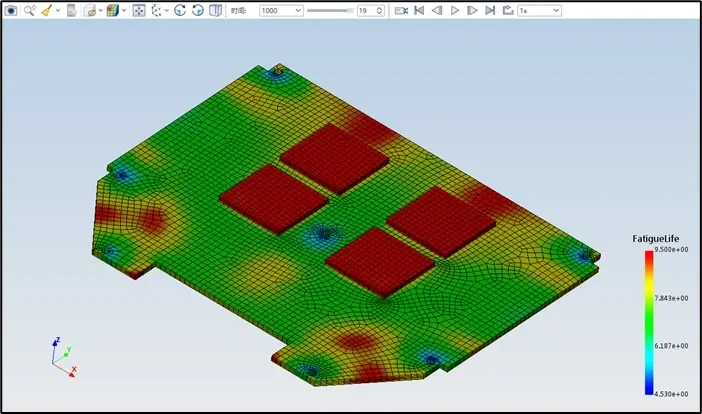
El primer paso es el diseño para la fiabilidad (DFR). El DFR es la fase de diseño que garantiza la fiabilidad de la placa de circuito impreso antes de construirla. Parte de este trabajo consiste en incluir buenas DFM en el diseño. Su fabricante de placas de circuito impreso puede ayudarle a elegir los tamaños correctos de las almohadillas y los paquetes de piezas. También puede proporcionarle normas de diseño para que pueda seguir la clase de IPC adecuada para su PCB. Otro paso de DFR consiste en utilizar herramientas de simulación para predecir dónde pueden producirse fallos en el diseño. Así podrá modificar el diseño antes de la fabricación.
Cada día llegan nuevas herramientas y métodos para tratar la fatiga por vibraciones y realizar análisis de vibraciones aleatorias. Aun así, es habitual probar los nuevos diseños con ensayos físicos de vibración y choque. Se fuerzan los fallos rápidamente aplicando vibraciones y choques superiores a los que sufre el producto en condiciones normales de uso. Esta prueba de vida altamente acelerada (HALT) es una parte importante del desarrollo de nuevos productos. Detecta posibles fallos relacionados con las vibraciones. Ayuda a garantizar que la estructura de la placa funcionará de forma fiable.