


Johdanto
A light-emitting diode (LED) is a solid-state semiconductor device that converts electrical energy into light. Compared with traditional incandescent lamps, LEDs have many clear advantages. These advantages include long service life, wide color range, strong durability, flexible design, simple control, and environmental protection. Because of these benefits, LEDs are widely considered one of the most promising light sources for the future.
Red, green, and blue (RGB) LEDs can be mixed to generate white light with a very wide color gamut. Because of this feature, RGB LEDs are very attractive for use in liquid crystal display (LCD) backlight systems. This type of backlight allows displays to become thinner, have a longer operating life, provide a higher dimming ratio, and show brighter and more vivid colors. At the same time, these displays are more environmentally friendly.
Because of these advantages, many research papers have been published on direct-lit LED backlight boards and edge-lit LED backlight boards. The world’s first LCD television that used RGB-LED mixed backlighting was released by Sony. This product achieved a very wide color reproduction range, reaching 105% of the National Television System Committee (NTSC) standard color gamut.
However, behind these research achievements, thermal issues still exist. During operation, LEDs generate heat. This heat causes a reduction in light output intensity and also leads to a shift in the dominant wavelength. These two effects change the color temperature of the display and result in variations in NTSC performance. In addition, excessive heat shortens the service life of the display. Therefore, in order to ensure image quality and long-term reliability, thermal management of the backlight system is extremely important.
To improve the thermal performance of an RGB-LED backlight system, two main approaches can be considered. The first approach is to improve the heat dissipation capability of a single LED. The second approach is to improve the heat dissipation capability of the LED array. As designers of an RGB-LED backlight system, we chose the second approach to solve the thermal problem.
To improve the thermal performance of an LED array system, there are also two common methods. One method is to use fans to increase the air flow speed around the backlight system. The other method is to reduce the thermal resistance from the LED junction to the ambient environment. Designing the backlight module on an economical and high thermal conductivity printed circuit board is a better solution.
At present, the widely used conventional insulated metal substrate (IMS) technology uses polymer or epoxy resin materials as the insulating layer. This technology requires special surface treatment of the metal base. In addition, the minimum thickness of the insulating layer is usually about 75 micrometers. This thickness increases the overall thermal resistance of the IMS board. Moreover, under high-temperature conditions, traditional IMS boards may suffer from delamination between the insulating layer and the metal base.
In this paper, we use magnetron sputtering technology to fabricate a new type of insulated metal substrate PCB. A chemically formed insulating layer with a thickness of 30 to 35 micrometers is generated on the surface of an aluminum base. Then, the designed circuit is formed on the insulating layer using magnetron sputtering. This new insulated metal substrate PCB has excellent thermal performance and can also eliminate delamination or peeling problems under high-temperature conditions.
Test results show that the thermal resistance of the new insulated aluminum substrate board is 4.78°C/W, while the thermal resistance of a traditional polymer-insulated aluminum substrate board is 7.61°C/W.
Magnetron Sputtering Technology
Basic Sputtering Process
Sputtering is a vacuum process used to deposit materials such as metals, ceramics, and plastics onto a surface to form a thin film. The basic sputtering process works as follows.
Electrons collide with inert gas atoms, usually argon, and ionize them. These high-energy ions are accelerated by an electric field and bombard the target material that is to be deposited. Because of this strong bombardment, atoms are ejected from the surface of the target material. Under the influence of the electric field, these atoms finally deposit on the surface of the substrate and form an atomic thin film. The thickness of this thin film depends on the sputtering time.
A conventional polymer-insulated metal substrate PCB typically consists of a copper layer, adhesive layer, polymer insulating layer, LED chip, adhesive, and aluminum base. In contrast, magnetron sputtering introduces an additional magnetic field into the process.
Magnetron Sputtering Process
The full magnetron sputtering process differs from basic direct current sputtering mainly because a strong magnetic field is applied near the target area. This magnetic field forces electrons to move along the magnetic field lines near the target surface instead of being attracted toward the substrate.
Compared with basic sputtering, magnetron sputtering offers three major advantages. First, the plasma region is confined near the target material and does not damage the forming thin film. Second, the electron path length becomes longer, which increases the probability of ionizing argon atoms. As a result, more target atoms are ejected, and the sputtering efficiency is improved. Third, the thin films produced by magnetron sputtering contain fewer impurities, which ensures high film quality.
Design of Anodized Insulated Aluminum Substrate PCB
The anodized insulated aluminum substrate PCB consists of three layers: the aluminum base layer, the anodized insulating layer, and the metallization layer. The metallization layer itself consists of three thin films, which are the base film, the conductive film, and the solderable film.
Aluminum Base Layer
The aluminum base layer forms the foundation of the PCB. When selecting aluminum material, two factors must be considered. First, the aluminum must have sufficient mechanical strength and good machinability. Second, it must be suitable for anodization and insulation treatment. Under certain conditions, the aluminum base can also be processed into a fin-shaped structure to further improve heat dissipation.
Anodized Insulating Layer
The anodized insulating layer is formed through a special anodization process that creates a microporous structure. This microporous structure determines the electrical insulation performance of the layer. Depending on the processing technology used, the dielectric strength of this layer can range from 250 V to 3000 V.
Using photolithography or masking technology, the circuit pattern is formed on this layer. This design allows seamless integration between the base layer and the insulating layer. At the same time, the LED chips are directly mounted on this layer. As a result, the LED chip, PCB, and heat sink form a single integrated structure. This greatly improves the overall thermal performance of the PCB.
Metallization Layer
The metallization layer consists of a base film, a conductive film, and a solderable film. This layer must not only provide good electrical conductivity but also ensure strong adhesion between the metallization layer and the anodized insulating layer. The circuit is formed on this layer using magnetron sputtering technology.
The base film has a thickness between 0.1 and 0.15 micrometers. It is formed by sputtering metals such as chromium or titanium. The main function of the base film is to provide strong adhesion between the metallization layer and the anodized insulating layer. With magnetron sputtering, the adhesion strength can reach 1000 N/cm², which makes the bond very stable. In addition, the base film has excellent high-temperature resistance. Even at temperatures above 320°C for 10 seconds, no blistering or peeling occurs. Therefore, it is fully suitable for lead-free soldering processes.
The conductive film has a thickness between 1 and 2 micrometers. It is formed by sputtering copper, nickel, or copper-nickel alloys. This film serves two main purposes. One purpose is to carry a certain current density. The other purpose is to act as a buffer layer when deformation occurs due to differences in thermal expansion coefficients between the base film and the solderable film. This buffering effect helps maintain the stability of the entire metallization layer.
The solderable film has a thickness between 0.3 and 0.8 micrometers. It is formed by sputtering metals such as gold or silver, which have good thermal conductivity, electrical conductivity, and solderability. The main function of this layer is to facilitate soldering of electronic components, including LED chips.
Manufacturing Process Technology
The entire manufacturing process includes five steps, which can be grouped into three main stages. These stages include anodization of the aluminum base, circuit pattern formation on the anodized insulating layer using photolithography or masking, deposition of the base film, conductive film, and solderable film using magnetron sputtering, and finally screen printing and application of flux and solder mask.
Anodization of the Aluminum Base
First, the aluminum base undergoes surface degreasing and cleaning. Then it is placed into an electrolytic bath filled with an electrolyte. The electrolyte can be sulfuric acid or oxalic acid, depending on the required properties of the oxide layer and the process conditions. During anodization, the aluminum base acts as the anode. Key process parameters include electrolyte concentration, current density, and electrolyte temperature. To obtain a qualified anodized insulating layer, the anodization time must be carefully controlled.
Magnetron Sputtering Deposition
Before film deposition, the circuit pattern must be created on the anodized insulating layer using photolithography or masking technology. When photolithography is used, the anodized aluminum plate is coated with photoresist, exposed, and developed. Then it is mounted in a fixture without a mask. When masking technology is used, a mask plate is mounted on the fixture surface when clamping the anodized aluminum plate.
Post-Processing Steps
According to design requirements, flux and solder mask are applied to specific areas of the coated anodized aluminum substrate PCB to prepare it for electronic component assembly.
Thermal Resistance Calculation Method
Thermal resistance refers to the resistance of a heat-conducting material to heat flow from a heat source to a heat-absorbing device. Its unit is °C/W. Thermal resistance is defined as the temperature difference divided by the heat power transfer rate.
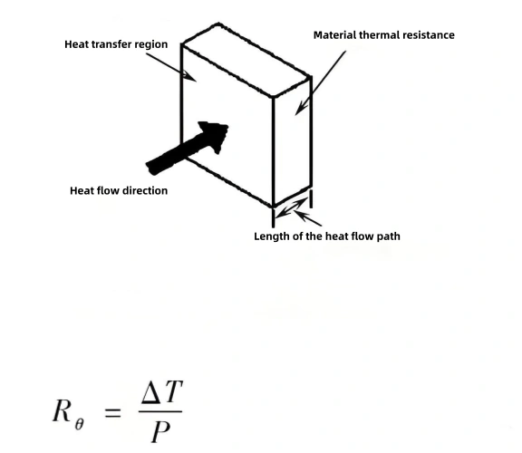
The thermal resistance between two points can be expressed as the temperature difference divided by the power dissipated between those points.
Thermal Resistance Measurement Method
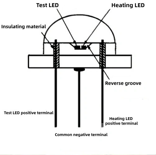
Several methods are commonly used to measure LED thermal characteristics. These include infrared thermal imaging, spectral methods, optical power methods, lead temperature methods, and electrical parameter methods. In this paper, an improved electrical parameter method is proposed.
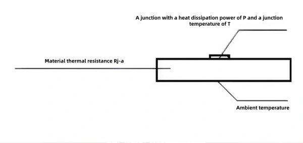
The thermal resistance between the junction and the ambient environment is calculated using the junction temperature, ambient temperature, and dissipated power. The junction temperature rise is linearly related to the change in forward voltage when the current is sufficiently small. Because the initial junction temperature is nearly equal to the ambient temperature, the junction-to-ambient temperature difference can be obtained directly.
By combining the relevant equations, the junction-to-ambient thermal resistance can be calculated. In practice, optical power is very small compared with electrical power, so it can be neglected.
The measurement procedure includes selecting a high-power LED as a heating source, using a standard LED as a test device, electrically isolating them, measuring voltage changes before and after heating, calculating temperature rise, determining dissipated power, and finally calculating thermal resistance.
Thermal Resistance Results of Anodized Insulated Aluminum Substrate PCB
Using the described method, the thermal resistance of both conventional polymer-insulated metal substrate PCBs and anodized insulated aluminum substrate PCBs can be calculated. In addition to overall thermal resistance, the thermal resistance of each individual layer is also measured.
The thermal resistances of different layers are connected in series. The total thermal resistance is the sum of the resistances from the junction to the metal layer, from the metal layer to the substrate, and from the substrate to the ambient environment.
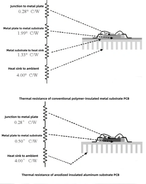
The results show that the thermal resistance of the anodized insulated aluminum substrate PCB is 59.2% lower than that of the conventional polymer-insulated metal substrate PCB. This improvement is mainly due to two factors. First, the conventional PCB has one more structural layer than the anodized PCB. Second, the anodized insulating layer is much thinner and has much better thermal conductivity than the polymer insulating layer.
Päätelmä
Thermal management is a critical issue in the development of RGB-LED backlight systems. In this study, a new type of anodized insulated aluminum substrate PCB is developed, and an improved electrical parameter method for thermal resistance measurement is proposed.
Compared with conventional polymer-insulated metal substrate PCBs, the anodized insulated aluminum substrate PCB has several advantages. There is no mechanical gap between the anodized insulating layer and the aluminum base, which improves overall mechanical strength. The three-layer metallization structure formed by magnetron sputtering provides strong adhesion of at least 1000 N/cm², which further enhances mechanical stability. In addition, the reduced number of layers and thinner insulating layer significantly lower the overall thermal resistance by 59.2%.
Because of these advantages, anodized insulated aluminum substrate PCBs are more suitable for use in RGB-LED backlight systems than conventional polymer-insulated metal substrate PCBs.

