1. Recent PCB Leakage Issue Overview
We recently faced a PCB leakage issue. The product is low-power. The whole device normally draws microamp-level (µA) current. After normal-temperature aging for some time, we found its power consumption rose. Some samples even reached milliamp-level (mA).
We carefully ruled out component faults. In the end we found a 5 V node. When the product was in sleep, this node should be 0 V, but it had about 1.8 V drop.
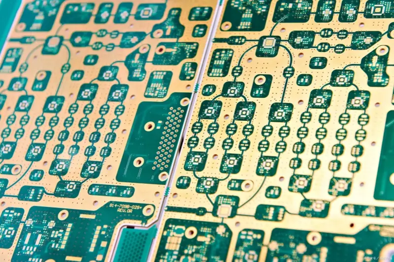
We carefully cut PCB traces. To our surprise, two vias that had no electrical connection on the PCB could be measured and showed a resistance of several hundred ohms between them. We checked the design files. It is a two-layer board. Via spacing and pad spacing > 6 mil. Hole-wall spacing > 18 mil. This design is normal for standard drilling in the PCB industry.
We removed the solder mask to rule out conductive contamination on the mask or via surface. The measured resistance between the vias still existed. We could not explain it for a while. Then we discovered the leakage was caused by the “CAF effect.”
2. What is CAF
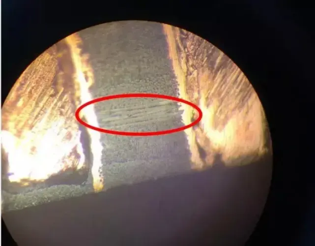
CAF means Conductive Anodic Filamentation. It is a leakage behavior inside a PCB where copper ions move from the anode (higher voltage) along microcrack channels between glass fibers toward the cathode (lower voltage). During this process, copper and copper salts cause leakage.
In the image, after grinding two adjacent vias lengthwise and looking at them under an electron microscope at 100×, the laminate looks dark. The bright gold areas are copper. You can see copper spots and copper filaments between the two vias.
3. How CAF forms (mechanism)
Normal fr4 PCB laminate is made by weaving glass fibers into cloth, then wetting with epoxy resin and semi-curing. If adhesion between resin and glass fiber is poor, or resin does not fully wet the glass, gaps can appear between them. During mechanical processing such as drilling, tangential pull and axial shock can further damage resin bonding. This can loosen or separate fiber bundles and create gaps.
When the environment is hot and humid, adhesion between epoxy and glass fiber degrades more. Silane coupling agents on the glass fiber surface can hydrolyze. This creates paths along the glass-fiber reinforcement that allow electron migration.
Given these conditions, if two nearby vias have a potential difference, copper at the higher-voltage anode can oxidize into copper ions. Under the electric field, copper ions move toward the lower-voltage cathode. During migration, they combine with impurity ions in the laminate or with OH– to form insoluble conductive salts, which deposit. As a result, the electrical spacing between the two insulating vias falls sharply. In severe cases, they can even form a direct conductive path and short.
Reactions at the anode and cathode (as observed):
Anode:
Cu → Cu²⁺ + 2 e⁻
H₂O → H⁺ + OH⁻
Cathode:
2 H⁺ + 2 e⁻ → H₂
Cu²⁺ + 2 OH⁻ → Cu(OH)₂
Cu(OH)₂ → CuO + H₂O
CuO + H₂O → Cu(OH)₂ → Cu²⁺ + 2 OH⁻
Cu²⁺ + 2 e⁻ → Cu
4. Notes from our experience
Before we knew the cause was CAF, we were baffled by resistance between two insulated vias. After searching the literature, we found many peers have suffered the same problem. CAF has become a notable reliability issue in the PCB industry.
5. How to prevent or reduce CAF
Improve the laminate resistance to CAF. For PCB substrate process, raise material ion purity. Use low-moisture-absorption resins. Ensure the glass cloth is fully wetted by resin and bonds well.
Be careful with drilling or laser via processes. Drilling or laser can produce high local heat. If the temperature exceeds the board’s Tg, resin can melt and form residue. Residue on hole walls can cause poor contact during plating. Therefore, remove residue before plating. Note: soaking during residue removal can erode through-holes and may cause copper contamination, which can make later copper migration easier.
Increase via-to-via spacing in PCB 설계. Also, CAF channels usually follow the same glass-fiber bundle. Staggering or offsetting neighboring vias helps reduce CAF risk.
Clean PCBA surfaces. For example, use a high-pressure air gun to remove dust and avoid impurity residues that could cause unwanted electrochemistry. Apply a conformal coating to the PCBA surface to prevent moisture ingress, especially in hot and humid environments.