


Open and short circuits in PCB traces are problems that almost every PCB manufacturer meets almost every day. These problems keep production and quality staff busy. They cause missed shipment quantities, extra rework, delivery delays, and customer complaints. These are hard problems in the industry. I have over 20 years of work experience in the PCB 제조 industry. I have worked mainly in production management, quality management, process control, and cost control. I have gathered some experience in fixing PCB open and short circuits. I now write this down as a summary for colleagues to discuss. I hope production and quality staff can use this as a reference.
1. Classification of Main Causes of PCB Open Circuits
We first group the main causes of PCB open circuits into the following areas:
Now we list the causes and the ways to improve, by category:
2. Open circuits caused by exposed base material (foil scratch)
The copper-clad laminate (CCL) already has scratches before it enters storage.
The CCL gets scratched during the cutting process.
The CCL gets scratched by drill bits during drilling.
The CCL gets scratched during transport.
After electroless copper, when stacked, boards get surface foil dents because of wrong handling.
During production, when boards pass a horizontal machine, the surface foil gets scratched.
2.1 Improvement methods:
Before entering storage, the incoming CCL must be spot-checked by IQC (incoming quality control). Check the board surface for scratches and exposed base material. If you find damage, contact the supplier in time and take the correct action based on the situation.
If the CCL is scratched during cutting, the main reason is hard sharp objects on the cutting table. When the CCL rubs against the hard object, the copper foil is scratched and the base material is exposed. So clean the cutting table well before cutting. Make sure the table is smooth and that no hard sharp objects remain.
If the CCL is scratched by drill bits during drilling, the main reasons are worn collets or dirt inside the collet. A dirty or worn collet cannot hold the drill bit tightly. The drill bit may sit lower than the set length and the tool may not rise enough during moves. When the machine moves, the tip can scrape the copper foil and expose base material.
a) Replace collets according to the count of tool changes or when the collet shows wear.
b) Clean collets regularly by work instructions to make sure no dirt remains inside.
Boards scratched during transport:
a) When moving boards, workers may lift too many boards at once or the load may be too heavy. Then they drag the boards rather than lift them. The board corners and the board surface rub and get scratched.
b) When putting boards down, if they are not stacked neatly, people may push them hard to arrange them. This causes rubbing between boards and scratches.
After electroless copper or full-panel electroplating, boards may be scratched while stacked because of wrong handling:
When boards are stacked after electroless copper or after full-panel electroplating, many boards together create weight. When a stack is set down, the board corners may hit down and with gravity and speed they create a strong impact on board surfaces. This can scratch the surface and expose the base material.
Production boards get scratched when passing a horizontal machine:
a) The stop plate on the sanding or grinding machine may touch the board surface. The plate edge may be uneven and may have sharp objects. When the board passes, the surface gets scratched.
b) A stainless steel drive shaft may be damaged and form a sharp point. When the board passes, this point scratches the copper and exposes the base.
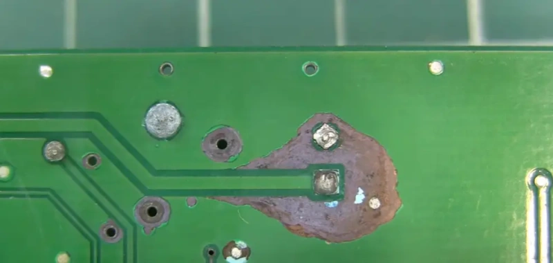
In summary, scratches that expose base material after electroless copper are easier to find on traces if they show as open lines or gaps. But if the scratch happens before electroless copper, then electroless copper can deposit copper over the scratch. The copper foil on the trace will be much thinner at that place. Later in open/short tests this is hard to find. When the customer uses the board, a high current may burn the trace and cause an open. The hidden quality risk and the economic loss can be large.
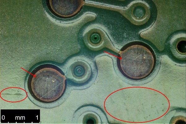
3. Open circuits caused by lack of hole plating (no hole plating)
No hole plating during electroless copper.
Oil left in holes causes no hole plating.
Excessive micro-etch causes no hole plating.
Bad plating causes no hole plating.
Drill bit burns holes or dust blocks holes and cause no hole plating.
3.1 Improvement measures:
No hole plating during electroless copper:
a) Hole conditioner problem: If the hole conditioner chemical balance is wrong or the solution is bad, the hole wall electric properties do not change as needed. The hole conditioner is to adjust the electrical property of the insulating base on the hole wall, so that palladium ions adsorb well and the electroless copper can fully cover. If the hole conditioner concentration is unbalanced or it has expired, no hole plating can happen.
b) Activator: The activator main components include palladium (Pd), organic acids, stannous ions, and chlorides. For palladium to deposit evenly on the hole wall, many parameters must be controlled. For our activator example:
i) Keep temperature at 35–44°C. If the temperature is too low, palladium density on the hole wall is low and electroless copper does not cover fully. If temperature is too high, reactions go too fast and material cost rises.
ii) Keep concentration (measured by color or strength) at 80%–100%. If the concentration is low, palladium density is low and electroless copper does not cover fully. If the concentration is high, the reaction is too fast and material cost rises.
iii) During production, maintain the activator solution. If it is heavily contaminated, the palladium on the hole wall will be not dense and the later electroless copper will not cover fully.
c) Accelerator: The accelerator mainly contains organic acids. Its job is to remove adsorbed stannous and chloride compounds from the hole wall so the catalytic metal palladium is exposed for later reactions. For our accelerator, keep the chemical concentration at 0.35–0.50 N. If the concentration is too high, all palladium may be removed and later electroless copper will not cover fully. If the concentration is too low, the removal of stannous and chloride is poor and later electroless copper will not cover fully.
d) Control of the electroless copper parameters is the key for good hole coverage. Using the bath parameters we use:
i) Keep temperature at 25–32°C. If temperature is low, the bath activity is poor and no hole plating happens. If temperature exceeds 38°C, the reaction is too fast, copper ions release too fast, and copper particles appear on the panel surface. This causes rework or scrap. In that case filter the electroless copper bath immediately, or the bath may be wasted.
ii) Control Cu2+ at 1.5–3.0 g/L. If Cu2+ is low, bath activity is poor and hole plating is bad. If it exceeds 3.5 g/L, reaction is too fast and copper particles form on panel surfaces and cause rework or scrap. Then filter the bath immediately. Cu2+ control is mainly done by adding electroless copper A solution.
iii) Control NaOH at 10.5–13.0 g/L. If NaOH is low, bath activity is poor and hole plating is bad. NaOH control is mainly done by adding electroless copper B solution. The B solution contains stabilizer for the bath. Normally add A and B in a 1:1 ratio.
iv) Control formaldehyde (HCHO) at 4.0–8.0 g/L. If HCHO is low, bath activity is poor and hole plating is bad. If HCHO exceeds 8.0 g/L, reaction is too fast and copper particles form on the panel surface and cause rework or scrap. Then filter the bath immediately. HCHO control is mainly done by adding electroless copper C solution. Note that A solution also contains HCHO components. So when adding A, calculate the HCHO increase first.
v) Keep bath load at 0.15–0.25 ft²/L. If the load is too low, bath activity is poor and hole plating is bad. If the load exceeds 0.25 ft²/L, reaction is too fast and copper particles form and cause rework or scrap. Then filter the bath immediately. In production, the first tank should use a copper board to activate the bath. This helps later boards react well. It ensures dense electroless copper in holes and higher coverage.
Suggestion: To keep these parameters balanced and stable, use an automatic dosing machine to add A and B solutions to the electroless copper tank. This helps control chemical components better. Also use automatic temperature control to keep the electroless copper line temperature stable.
Wet film or ink left in holes causes no hole plating:
a) When screen printing wet film, print one board and then scrape the mesh. This makes sure the mesh does not have pooled ink. Normally this prevents wet film remaining inside holes.
b) When screen printing wet film, use mesh counts of 68–77T. If you use the wrong mesh, for example ≤51T, wet film may leak into holes. During developing the hole may not be clean. During plating the hole will not plate metal and you get no hole plating. If mesh is too high, the wet film may be too thin, and during plating the resist can be broken by current. This leads to many metal dots or even shorts between traces.
Excessive micro-etch (over-roughening) causes no hole plating:
a) If the board uses chemical micro-etch before line patterning, control the solution temperature, concentration, and time. Otherwise, if the copper in plated holes is thin, the micro-etch may dissolve the copper and cause no hole plating.
b) To improve layer bonding, pre-plating treatments use chemical micro-etching. So control micro-etch temperature, concentration, and time well. Otherwise this can also cause no hole plating.
No hole plating due to electroplating issues:
a) When the aspect ratio (thickness to diameter) is large (≥5:1), bubbles can form in holes. This is because vibration is not enough to make the air escape. Ion exchange cannot happen well. The hole then does not plate copper or tin well and you get no hole plating.
b) When aspect ratio is large (≥5:1), if pre-plating cleaning did not remove oxidation on the hole wall, during electroplating you get resistance to plating. The hole will not plate copper or tin well, or the plated copper/tin will be very thin. During etching the thin copper in holes can be removed and cause no hole plating.
Drill bit burns holes or dust blocks holes and cause no hole plating:
a) If drill-tool life is not set correctly or the drill bit is very worn (with chipping or not sharp), then friction during drilling makes heat. The hole wall burns and cannot be covered by electroless copper, so no hole plating happens.
b) If the dust extraction is weak or the engineering for dust removal is not optimized, dust can block holes during drilling. During electroless copper the blocked holes do not get copper and you get no hole plating.

