

















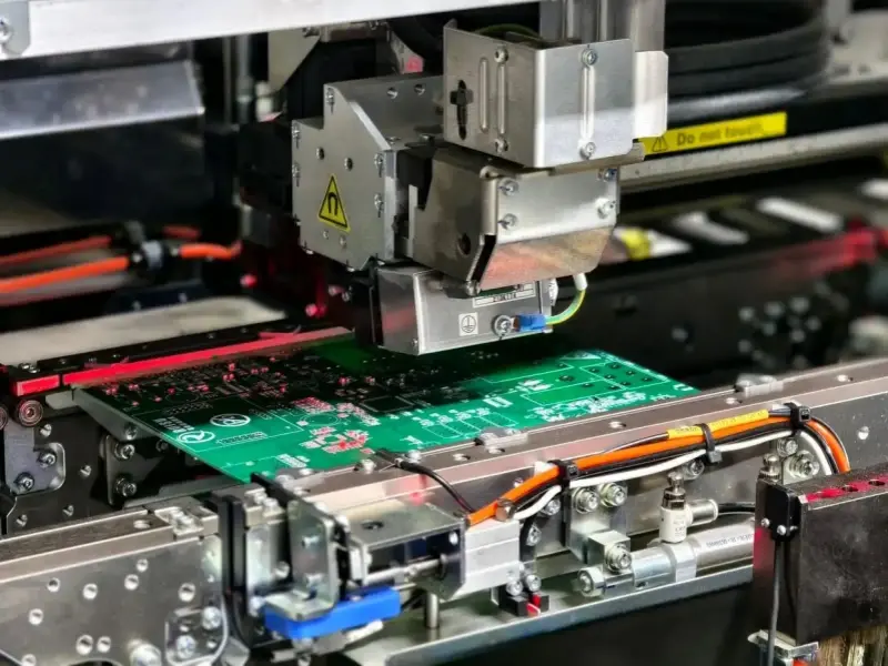
Prototype PCB assembly, in plain English, is the part where your PCB prototype becomes a working, testable board. A real PCBA. Components placed, soldered, powered up. Not just pretty Gerbers.
And yeah, this is where projects either start moving fast… or they quietly die.
Because a hardware project isn’t “done” when the schematic looks right. It’s not even “done” when the PCB comes back from fab and you hold it in your hand like a trophy. The truth is, you only learn the important stuff when it’s assembled and you can run current through it.
Here’s where prototype assembly fits in the typical flow:
Concept → schematic/layout → Proizvodnja tiskanih pločica → assembly → testing/validation → iteration → low-volume → production.
One quick expectation reset, because this trips people up. Prototypes are not about minimum unit cost. They’re about learning speed and risk reduction. You are paying to find problems early, before they become five-figure mistakes.
So when people say they want a “good prototype PCB assembly service,” they usually mean three things:
- Speed and lead time (quick turn that’s actually quick)
- Quality assurance (QA) (so you’re not debugging assembly defects all week)
- Real engineering support (someone who answers questions and catches issues before they ship you a mess)
If you’re looking for such a service, consider reaching out to FLJ PCB, who specialize in providing high-quality prototype PCB assembly services with fast turnaround times and excellent engineering support.
Prototype PCB vs production PCB assembly: what actually changes
Prototype and production PCB assembly can look similar on the surface. Same SMT machines, same reflow ovens, same solder paste. But the goals and the discipline around the process are different.
Prototype assembly goals:
- Validate the design
- De-risk the layout
- Confirm footprints, polarity, pin 1, orientation
- Prove the power tree and the basics
- Get something you can test and iterate on
Production assembly goals:
- Optimize yield and repeatability
- Lock the supply chain (AVL, alternates, lifecycle planning)
- Control cost per unit
- Scale test coverage and reduce escapes
- Make the build boring, predictable, and auditable
That difference in goals changes a bunch of practical things.
Process controls that usually change from prototype to production
In production, you’ll see more of this:
- BOM finalization with lifecycle checks and alternates already approved
- AVL (Approved Vendor List) and tighter sourcing rules
- Panelization designed for throughput, not convenience
- Tooling and fixtures (stencils, pallets, selective solder fixtures)
- Test coverage expands: ICT, FCT, maybe boundary scan
- Documentation maturity: work instructions, photos, torque specs, packaging specs, serialization
In prototypes, reality is messier:
- Partial substitutions happen because one part is out of stock
- Manual rework is normal, not an exception
- There are engineering holds while someone asks “is R17 rotated wrong or is the footprint wrong?”
- Schedules are higher mix, lower volume, more interruptions
Also, sometimes what you call a “prototype” is actually low-volume production. Like 200 units shipping to beta customers. That matters for quoting and test strategy, because now you care about consistency, traceability, and a minimum level of test coverage. If you treat that like a casual prototype build, you can end up with inconsistent units and painful field failures.
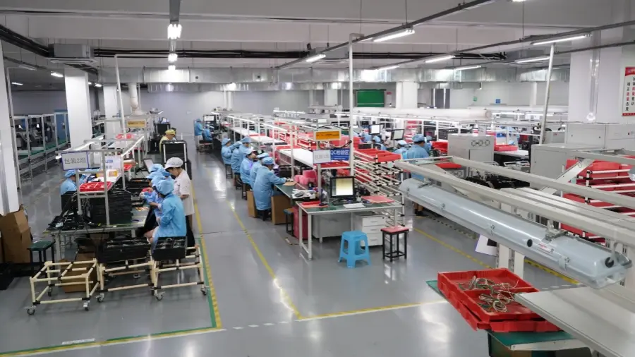
Before assembly: get the design and fab details right (DFM is the cheat code)
If you want speed and quality, the fastest win is boring. Do a quick DFM pass before you order assembly.
Because most prototype delays are not “the assembler is slow.” They’re “we have questions” questions. Missing centroid file. Ambiguous polarity. Wrong footprint. No fiducials. A QFN pad that needs a paste tweak. Stuff that could have been caught in an hour, now turning into days.
Files a prototyping assembler typically needs
If you send a clean package, quotes come back faster, and builds start faster. Usually they’ll ask for:
- Gerbers or ODB++
- Drill files
- IPC-356 netlist (often optional but helpful)
- BOM (with manufacturer part numbers, not just “10k resistor”)
- Centroid / pick and place file
- Assembly drawings (top and bottom, refdes, polarity, special notes)
- Schematic PDF
- Programming and test notes (if any)
- Any special handling notes (MSL, conformal coat, cleaning rules)
And yes, exports matter. Whether you use Altium Designer, Eagle, KiCAD, EasyEDA, OrCAD, Protel, whatever. Just make sure layer naming is sane, files aren’t missing, and your pick and place origin is correct. A surprising number of “prototype assembly errors” start with a weird export.
Key DFM checks that affect assembly speed and QA
These are the ones that keep showing up:
- Footprints: correct land pattern, correct pin 1, correct courtyard
- Polarity marks: diodes, electrolytics, LEDs, tantalums, IC pin 1, connectors
- Spacing and solder mask openings: fine pitch parts hate sloppy mask definition
- Fiducials: global and local, especially for fine pitch and BGAs
- Panelization: if the board is tiny or odd shaped, panelize it properly
- Tooling holes: for repeatable setup
- Paste apertures: QFN thermal pads, 0.4 mm pitch, via in pad rules
- Via in pad: if you do it, do it right (filled and capped when required), otherwise hello solder wicking
On standards language. People often say “IPC-9001” when they mean ISO 9001. IPC isn’t ISO. For assembly acceptability, you’re usually targeting IPC-A-610 (Class 2 or Class 3 depending on the product). If a vendor can’t speak clearly about this, that’s not automatically a dealbreaker for prototypes, but it’s a signal.
Prototype PCB fabrication essentials (what your assembler cares about)
Assembly quality is tied to fabrication quality more than people want to admit.
Your assembler cares about:
- Flatness (warped boards make placement and reflow painful)
- Završna obrada površine (ENIG, HASL, immersion silver, etc)
- Solder mask quality (registration, thickness, cleanliness)
- Drill accuracy (for THT, vias, and alignment)
- Kontrola impedanse (if you claim it’s controlled, it needs to be real)
- Overall consistency (because prototypes still need to be buildable)
Quick practical overview of PCB fabrication
A simplified version of the “printing” process from raw material to board looks like:
Substrate prep → photolithography → copper etching → drilling → plating → solder mask → silkscreen → electrical test.
Behind those words are a lot of parameters. Drilling can be mechanical or laser drilling, plating has multiple methods (through-hole plating, selective, finger plating, reel linkage selective), solder mask is applied for protection and durability, silkscreen has its own process controls. In real factories you’ll see very specific settings, like bonding pressure, scraper pressure, scraper angle, print speed, ink thickness, quiescence time. It’s not random. It’s process control.
For a deeper understanding of the different approaches in PCB fabrication such as subtractive vs MSAP, it’s essential to explore these methodologies further.
Common board types for prototypes and why they’re chosen
- Jednostrana štampana pločica: cheap, simple, fast. Great for basic circuits.
- Dvostrana tiskanica: still quick, more routing freedom.
- Multi-layer PCB: where most modern products live because of power and signal integrity.
- High-frequency PCB: when loss and dielectric properties matter.
- Tvrdo-fleksibilna štampana ploča: when mechanical packaging forces your hand.
For more information on the different types of PCBs and their design aspects, you can explore this comprehensive guide on PCB design.
Materials cheat sheet
- FR4: the default. General electronics.
- poliamid: flex circuits and higher heat tolerance.
- Metal-core substrate: thermal performance, LED boards, power modules.
If you choose exotic materials, it’s fine. Just understand you are trading lead time and cost for performance. Make it intentional.
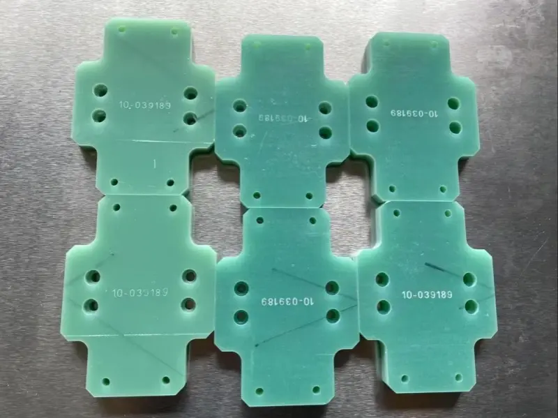
The prototype PCB assembly process (step-by-step, what happens on the floor)
Prototype assembly is basically a controlled sprint. Here’s what happens on the floor, and where things usually go right or wrong.
Step 1: Incoming inspection and kitting
- Verify PCB fab notes, stackup, finish, basic workmanship
- Count boards, check for damage
- Verify components vs BOM
- Provjeri MSL and storage requirements (moisture sensitive parts are not a suggestion)
If your parts show up in random zip bags with no labels, expect delays. Or errors.
Step 2: Solder paste printing
Stencil selection matters. Paste type matters. Aperture tuning matters.
And this is a frequent prototype failure point because your design might have:
- fine pitch pads
- big thermal pads
- uneven paste volume needs
A “generic” stencil can lead to bridging, tombstoning, or insufficient solder. Prototypes often need paste tweaks, especially on QFNs and tiny passives.
Step 3: SMT placement (pick and place)
Machine places components based on the centroid file. If your rotations are wrong in the file, the machine will confidently place wrong parts perfectly wrong. That’s why assembly drawings and a good centroid export are a big deal.
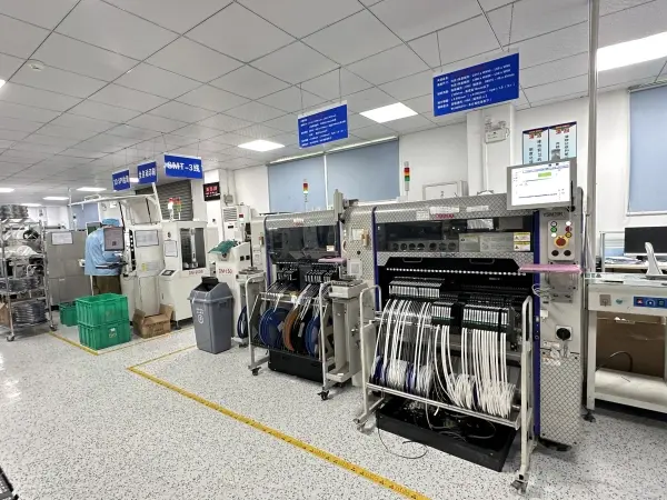
Step 4: Reflow soldering
Controlled heat profile. Enough soak, enough time above liquidus, correct peak. Too hot and you damage parts. Too cool and you get weak joints. Warped boards can cause opens under BGAs too, which is a special kind of pain.
Step 5: Through-hole assembly (if needed)
Connectors, transformers, big caps, anything with mechanical stress. This can be hand soldered, wave soldered, or selective soldered depending on volume and complexity.
Step 6: Rework and repair
Prototypes often include controlled rework. It’s normal.
- Hot air rework
- Drag soldering touch-ups
- BGA reball if needed (not always worth it on prototypes, but possible)
- Jumper wires, bodge wires, resistor swaps
The key word is controlled. Rework should be documented, not improvised in silence.
Step 7: Cleaning and conformal coat (if required)
Sometimes you need cleaning for high impedance analog or high reliability. Sometimes you need conformal coat for environment. But in early validation, you often want to avoid coating until the design is stable. Coating hides rework and makes debugging miserable.
How speed actually happens during prototype builds
It’s not magic, it’s parallel work:
- Run fab and sourcing in parallel
- Freeze critical parts early (MCU, PMIC, RF front end)
- Reduce build variants (one BOM, one rev, one set of options)
- Be explicit about acceptable substitutions
Speed: what “quick turn prototype PCB assembly” really depends on
Lead time is usually a stack of four buckets:
- PCB fabrication time
- Component sourcing time
- Assembly queue time
- Testing time
You can only go as fast as the slowest bucket.
Turnaround ranges are variable on purpose:
- Same day / 24 to 72 hours for very simple builds with in-stock parts, standard stackups, minimal testing.
- 1 to 3+ weeks when parts are constrained, the design is dense, or you need programming and real functional testing.
What accelerates builds
- In-stock components, or you provide consigned parts
- Alternates already approved
- Standard stackups and finishes
- No controlled impedance requirement
- Consistent, correct footprints
- Clear assembly notes and polarity/orientation callouts
What slows builds
- BGAs and 0.4 mm pitch parts
- Rigid-flex builds
- High-frequency materials
- Controlled impedance with coupons
- Special stencil requirements
- Programming, firmware loading, and debug loops
- Custom test fixtures
Practical checklist for faster quotes and faster builds
- Complete BOM with MPNs
- PCB fab drawing and stackup notes
- Polarity and orientation notes
- AVL if you have it
- Acceptable substitutes listed
- Target ship date and quantity
If you do that, you remove most of the back and forth.
Cost drivers in prototype PCB assembly (and how to lower cost without lowering quality)
Prototypes cost more per unit because you’re paying for setup and complexity that production spreads across thousands of units.
Common cost drivers:
- Setup and NRE
- Stencil cost
- Programming setup
- Low-volume inefficiency (high mix, stops and starts)
- Higher rework rate, because prototypes
Typical cost line items you’ll see:
- Proizvodnja tiskanih pločica
- Stencil
- SMT and THT labor
- Component cost (and shortages can spike this)
- Expedited fees
- Rework
- Testing (flying probe, FCT)
- Shipping
Ways to reduce cost intelligently
- Design for assembly using standard packages where possible
- Consolidate the BOM (ten resistor values when you could use four is real money)
- Avoid exotic finishes and materials unless you need them
- Approve alternates early
- Order extra passives. Seriously. They disappear.
- Panelize when appropriate (and when the assembler agrees it helps)
The tradeoff is simple. Cheapest quote vs on-time working boards. If your goal is learning speed, paying for QA and support is often cheaper than burning a week debugging bad solder joints.
Quality assurance for prototypes: the inspection stack you actually want
For prototypes, you want QA that finds real issues without turning the build into a slow, bureaucratic production line.
AOI (Automatska optička inspekcija)
AOI is the baseline for SMT boards. It catches:
- Missing components
- Wrong components (sometimes)
- Polarity/orientation errors
- Solder bridging and insufficient solder on visible joints
What AOI cannot do well:
- Hidden joints (BGA, bottom terminated parts)
- Some kinds of opens under packages
- Electrical performance
When X-ray testing matters
If you have BGAs, QFNs, or anything with hidden solder joints, X-ray is the difference between confidence and guessing. An Automatic X-ray Inspection System can validate:
- Voiding
- Bridges under packages
- Opens
- Ball alignment issues
Not every prototype build needs X-ray, but if your design depends on hidden joints, skipping X-ray can be a false savings.
Functional Testing (FCT)
FCT is the real “did we build it right?” check.
Powering the board, loading firmware, running basic bring-up scripts, verifying rails, IO, comms. Even a simple smoke test is better than nothing.
You’ll also hear teams mention other test language, sometimes loosely:
- Adjacency testing (shorts and spacing issues)
- Flip testing (a practical orientation and polarity check)
- Continuity and comparative testing
Acceptance criteria and documentation
Have a clear expectation. IPC-A-610 class, what defects are acceptable, and what data you want back:
- Test reports
- AOI images (on request)
- X-ray images (on request)
If a vendor can provide this without acting like you’re being difficult, that’s a good sign.
Support: what “real support” looks like in prototype PCBA
Support is not “our portal is nice.” Support is what happens when something is unclear and the clock is ticking.
Good support usually includes:
- DFM feedback before the build starts
- Fast clarification questions that are actually specific
- A clear substitution approval workflow
- Photo updates if something looks off
- Root-cause notes when issues happen, not vague excuses
Engineering communication loops
The most common prototype questions are predictable:
- “Your diode polarity marking is unclear, confirm orientation.”
- “U7 pin 1 marker conflicts with silkscreen.”
- “R34 footprint doesn’t match the MPN package.”
- “Missing refdes on bottom side drawing.”
- “BOM calls for part that is NRND, approve alternate?”
A good partner asks fast, and doesn’t build until it’s resolved. A bad partner guesses.
Component sourcing support
Shortages are normal now. Support means:
- Recommending alternates that make sense
- Handling partial shipments without losing traceability
- Offering turnkey vs consigned builds depending on what you need
Rework and iteration friendliness
Prototype work means ECOs. Rev A to Rev B to Rev C. A supportive assembler documents:
- Patch wires and bodges
- Component swaps
- What changed and why
- How to replicate the fix on the next build
That is “real support.” Not just shipping boards.
Choosing a prototype PCB assembly partner (certs, capabilities, and red flags)
Picking a prototype partner is a little like picking a debug partner. You want the one that tells you the truth quickly.
Capabilities checklist
- SMT and THT
- Fine pitch and BGA capability
- Rigid-flex experience (if you need it)
- Controlled impedance handling (if you need it)
- Programming and firmware loading
- Conformal coat (if you need it)
- Rework capability
QA and test checklist
- AOI in-house
- X-ray access for hidden joints
- Flying probe or equivalent electrical test option
- Documented process control and traceability
- Willingness to share build notes and reports
Geography tradeoffs: China PCBA vs local
This is not a moral decision. It’s a schedule decision.
China PCBA can be cost-effective and fast when the pipeline is smooth, and many reputable providers run very capable facilities. Local can be faster for iteration loops, easier communication, simpler shipping risk, and sometimes better for IP comfort.
So how do you decide?
- If you need rapid iteration and lots of back and forth, local often wins.
- If your design is stable and you want cost efficiency, overseas can be great.
- If your schedule is tight, shipping risk matters more than you think.
You’ll see reputable prototyping brands in the market, like PHILIFAST , and others. The key is not the name, it’s the behavior: how they quote, how they question, how they handle problems.
Vendor evaluation that actually predicts the future
- Ask for sample build photos
- Ask what their substitution process looks like
- Ask what QA steps are standard on prototype builds
- Pay attention to responsiveness during quoting
Quoting behavior is usually support behavior later. People don’t suddenly become organized after you pay.
A practical “send-to-assembly” checklist (so your first build doesn’t stall)
If you want your first build to not stall in an email thread, here’s a checklist that works.
Design and package checks
- Clear polarity markers and pin 1 indicators
- Reference designators on silkscreen (readable, not under parts)
- Test points for key rails and interfaces
- Fiducials (global and local)
- Keepouts and courtyard spacing
- Solder mask expansion appropriate for your fab
- Silkscreen clarity (especially on black or dark solder mask)
Fab checks
- Correct stackup and copper weight
- Surface finish choice is intentional
- Solder mask color choice doesn’t sabotage readability
- Drill file accuracy and hole size callouts
- Impedance notes if needed, and specify tolerance
Assembly package
- BOM with MPNs and acceptable alternates
- Centroid / pick and place
- Assembly drawings (top and bottom)
- Programming instructions
- Special handling notes (MSL, baking, ESD)
- Target quantity plus spares
Testing plan
- Minimum electrical test (even basic continuity) plus a functional smoke test
- Define pass/fail
- Define what data you want back (logs, measurements, photos)
Logistics and Controls
- Shipping addresses and preferred carrier
- Incoterms if applicable
- Decide turnkey vs consigned parts
- Revision control naming (Rev A, Rev B, etc) and ensure everyone uses the same file set
Wrapping Up: Speed is Useless Without QA and Support
Prototype PCB assembly only looks like a race. It’s actually a loop.
The best prototype outcome is not “we got boards fast.” It’s “we got boards fast that we can trust.” That means fast turnaround, layered inspection and testing, and responsive engineering communication when something is ambiguous.
Prototype boards are for learning. Build, test, fix, repeat. Then when you transition to low-volume and production, you tighten DFM, lock sourcing, and expand test coverage. That’s how projects survive the jump.
Next step if you’re about to send a build out: prepare the file package and the checklist above, then request quotes with a clear lead time target and clear test requirements. You’ll get better answers, and usually better boards.
Final Thoughts: How to Choose the Right PCB Prototype Partner for Your Next Project
PHILIFAST vs Typical PCB Prototype and PCBA Providers
1. Service that feels like an engineering partner, not a ticket system
A lot of PCB companies can take an order. The difference is how PHILIFAST supports the messy parts. DFM feedback, quick clarifying questions, and practical suggestions before the build starts. When you are on Rev A and everything is urgent, that responsiveness is the product.
2. Flexibility during prototyping (where reality changes daily)
Many established providers are optimized for stable production, which is great later. PHILIFAST is positioned for prototype reality: substitutions, partial builds, fast rework, ECO driven changes, and small batch assembly without forcing you into a rigid process that only works when everything is perfect.
For instance, their BGA montaža service showcases this flexibility perfectly.
3. Production capability that still respects prototype speed
Some prototype shops are fast but can’t scale. Some production shops can scale but are slow to engage on prototypes. PHILIFAST aims to bridge that gap, supporting quick turn prototypes while also having the manufacturing depth to carry a project into low-volume and beyond without you needing to re-qualify an entirely new supplier.
Their SMT montaža service exemplifies their ability to maintain speed while ensuring quality during production runs.
4. Quality control you can actually see
When comparing vendors, look for proof, not slogans. PHILIFAST emphasizes practical QC steps like AOI, access to X-ray for hidden joints when needed, and traceable build documentation. That helps you separate design bugs from assembly defects which is basically the whole game in prototyping.
5. One-stop manufacturing support that reduces handoffs
With many PCB companies, you end up coordinating fab at one place, assembly at another (like THT PCB assembly), components somewhere else
Često postavljana pitanja
What is prototype PCB assembly and why is it critical for hardware projects?
Prototype PCB assembly is the process where your PCB prototype becomes a functional, testable board with components placed and soldered. It’s critical because this is where you truly validate the design by powering up the board and running tests. Most hardware projects either accelerate or fail at this stage since schematic correctness or fab completion alone don’t guarantee a working product.
How does prototype PCB assembly differ from production PCB assembly?
While both use similar equipment like SMT machines and reflow ovens, prototype assembly focuses on validating the design, de-risking layout, confirming footprints and polarity, and enabling testing and iteration. Production assembly emphasizes optimizing yield, locking supply chains, controlling costs per unit, expanding test coverage, and making the build repeatable and auditable.
What are the key expectations from a good prototype PCB assembly service?
A good prototype PCB assembly service typically delivers: 1) Speed and quick lead times to accelerate development cycles; 2) Quality assurance to minimize debugging of assembly defects; and 3) Real engineering support to answer questions and catch issues before shipping, ensuring a reliable prototype build.
What files and documentation should be prepared before sending a PCB for prototype assembly?
To ensure fast quotes and smooth builds, provide a clean package including Gerbers or ODB++, drill files, IPC-356 netlist (optional but helpful), a detailed BOM with manufacturer part numbers, centroid/pick-and-place file, top/bottom assembly drawings with reference designators and polarity marks, schematic PDF, programming/test notes if any, plus special handling instructions like moisture sensitivity levels or conformal coating requirements.
What are common Design for Manufacturability (DFM) checks that impact prototype PCB assembly quality and speed?
Key DFM checks include verifying correct footprints with accurate land patterns and pin 1 orientation; ensuring clear polarity markings for diodes, electrolytics, LEDs, tantalums, ICs; proper spacing and solder mask openings especially for fine pitch parts; inclusion of global and local fiducials for precise component placement; and appropriate panelization for small or irregularly shaped boards.
How should low-volume production runs be treated differently from prototypes in PCB assembly?
Low-volume production (e.g., 200 units for beta testing) requires more consistent processes than casual prototypes. It demands attention to consistency across units, traceability through serialization or documentation, finalized BOMs with approved vendor lists (AVL), expanded test coverage like ICT or FCT, and stricter quality controls to avoid field failures that could arise from treating them as informal prototypes.