

















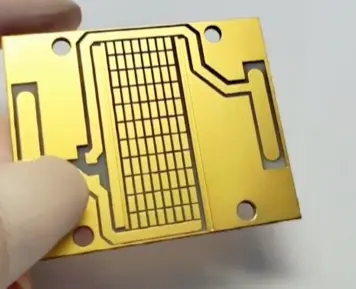
Properties of ceramic PCB
Mechanical properties (how circuit traces are formed)
b. They are easy to machine. They keep accurate dimensions. They can be made into many layers.
c. Their surface is smooth. They do not warp, bend, or show small cracks.
Električna svojstva
b. They have low dielectric constant and low dielectric loss. This helps signals pass with less loss.
c. Their performance stays stable at high temperature and high humidity. This helps ensure reliability in hard use conditions.
Thermal properties
b. Their thermal expansion coefficient can match related materials, especially silicon. This match reduces stress when parts heat and cool.
c. They have good heat resistance. They stay stable at high temperature.
Other properties
b. They do not absorb moisture. They resist oil and chemical attack. They release little radiation.
c. The materials used are harmless and not toxic. Their crystal structure does not change in the working temperature range.
d. Raw materials are abundant. The technology is mature. They are easy to make and the price is low.
Methods to make ceramic substrates
- Stack layers – hot press – remove binder – fire the base sheet – form circuit patterns – fire the circuit.
- Stack layers – print the circuit pattern on the surface – hot press – remove binder – co-fire.
- Print circuit pattern – stack – hot press – remove binder – co-fire.
Metallization of ceramic PCB
a. Thick film method:
b. Thin film method:
c. Co-firing method:
■ It can form very fine circuit lines and it is easy to make many layers, so high density wiring is possible.
■ Because the insulator and the conductor are formed together, hermetic sealing in packages is possible.
■ By choosing the right composition, forming pressure, and sintering temperature, the sintering shrinkage can be controlled. Especially when a substrate with zero in-plane shrinkage is made, this opens up use in BGA, CSP, and bare chip high-density packaging.
Types of ceramic substrates
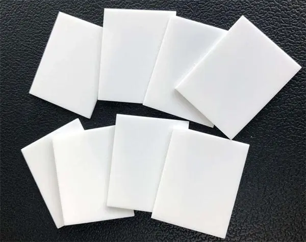
Alumina substrate (Al₂O₃)
b. Making: Al₂O₃ ceramics are usually formed by stacking unfired sheets. A binder like polyvinyl butyral (PVB) is often used. The firing temperature varies with added sintering aids, and is usually 1550–1600°C. Metalization methods for Al₂O₃ are mainly the thick film and co-firing methods. The pastes and the process technology are mature. They meet many application needs today.
c. Applications: Substrates for hybrid integrated circuits, LSI package substrates, and multilayer circuit substrates.
Mullite substrate (3Al₂O₃·2SiO₂)
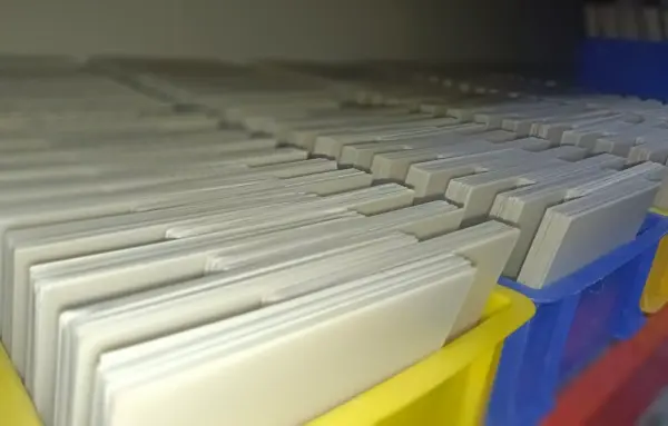
Aluminum nitride substrate (AlN)
b. Making: The same forming methods used for Al₂O₃ substrates can be used for AlN. The most used route is stacking unfired sheets. For this, AlN powder, organic binders, solvent, and a surfactant are mixed to make a ceramic slurry. The slurry is tape cast, stacked, hot pressed, debindered, and then fired to make the AlN substrate.
c. AlN substrate features: AlN has thermal conductivity more than ten times that of Al₂O₃. Its coefficient of thermal expansion (CTE) matches silicon. Compared with Al₂O₃, AlN has higher insulation resistance and higher breakdown voltage. Its dielectric constant is lower. These features make AlN very valuable for package substrates.
d. Applications: Used for VHF band power amplifier modules, high power devices, and laser diode substrates.
Silicon carbide substrate (SiC)
b. Making: SiC has very high chemical and thermal stability, so normal firing methods make it hard to densify. Sintering aids and special firing methods are needed. Vacuum hot pressing is commonly used.
c. SiC features: A key feature is its very large thermal diffusion coefficient. It can even be larger than copper. Its thermal expansion is closer to silicon. But SiC has some downsides. Its dielectric constant is relatively high and its breakdown voltage is not as good as some other ceramics.
d. Applications: SiC substrates are used where high heat spreading is needed and voltage is not high. They are used for VLSI heat-sinking packages, high speed and high integration logic LSI with heat sinks, large computers, and laser diode substrates for optical communications.
Beryllia substrate (BeO)
Comparison of some ceramic materials and substrate types
High temperature co-fired ceramic multilayer (HTCC)
Low temperature co-fired ceramic PCB(LTCC)
Thick film ceramic substrate (TFC)
Direct bonded copper ceramic PCB(DBC)

Direct plated copper ceramic PCB(DPC)
Notes on use and selection
Manufacturing tradeoffs and practical points
Co-firing vs post-firing metallization
Typical process flow examples (short summary)
- For co-fired multilayer substrate: make ceramic slurry, tape cast, drill vias in green tape, print conductor pastes by screen, stack tapes, press and debind, and then fire. After firing, do final processing like pad metallization and circuit etching if needed.
- For thick film on ceramic: use fired ceramic substrate, screen print conductor and resistor pastes, fire at 700–800°C, then trim resistors and add final metal pads.
- For DPC: clean ceramic, deposit Ti/Cu seed by sputter, pattern photoresist, etch seed to make pattern, electroplate to grow copper, strip resist, and final clean.
Sažetak
Često postavljana pitanja
The most common are alumina (Al₂O₃) for general use and aluminum nitride (AlN) for higher thermal conductivity; other specialized ceramics (e.g., silicon carbide) are used for niche high-power or high-temperature needs.
Ceramic PCBs are made by processes such as thick-film printing, thin-film deposition, laser machining, and metalization (copper or silver), followed by firing and finishing.
Key advantages: much better thermal conductivity (heat dissipation), lower coefficient of thermal expansion (CTE), high-temperature tolerance, and excellent electrical insulation—making them ideal for LEDs, power electronics, and RF/high-frequency applications.
Yes—material costs and specialized processes (firing, laser machining, metallization) typically make ceramic PCBs pricier than standard FR-4; however, for high-power or high-reliability designs they can reduce system costs by improving performance and lifetime.
Yes. Ceramic substrates offer stable dielectric properties and low loss at high frequencies, making them a strong choice for RF and microwave circuit components.
Choose alumina for cost-effectiveness and general use; choose AlN when you need higher thermal conductivity and better thermal management for high-power applications. Your choice should reflect thermal, mechanical, and budget requirements.