
PCB Manufacturing Capabilities
FLJ PCB manufactures bare circuit boards for prototype and production builds. Compare materials, copper, drilling and finishing options, then send the files you have for an engineering review.
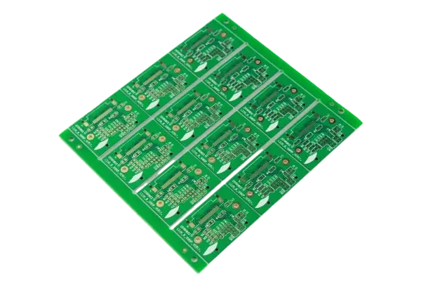
Board constructions for different products
Our fabrication scope includes rigid FR4, multilayer, HDI, flexible, rigid-flex, high-frequency, metal-core and ceramic boards.
Choose the construction around the electrical and mechanical tasks of the product. A multilayer board provides routing space and reference planes; a flex section connects moving or closely spaced assemblies; a metal base supports a defined thermal path. The specification brings these decisions together.
FLJ PCB connects fabrication with assembly, component sourcing, programming and testing when a project needs a complete PCBA. This page describes bare-board capability. Assembly package handling and product integration are covered separately.
Rigid PCB process overview
Published process ranges are matched to your material and construction during engineering review.
| Funktion | Published general capability | Context |
|---|---|---|
| Lag | 1–30 | General rigid-board scope |
| Finished copper | Outer up to 8 oz; inner up to 6 oz | Copper weight affects routing |
| Minimum board size | 5 × 5 mm | Small boards use panel preparation |
| Interlayer alignment | ≤3 mil | Multilayer registration |
| Mechanical finished holes | 0.10–6.2 mm | Finished and drill diameter differ |
| Impedance tolerance | ±5 Ω below 50 Ω; ±10% at ≥50 Ω | Defined stack-up and target |
| Thickness tolerance | ±0.1 mm at ≤1.0 mm; ±10% above 1.0 mm | General process table |
Copper weight and trace spacing
Published line and space values change with copper weight. Heavy-copper routing needs a different allowance from a fine-line signal board.
Review current, temperature rise, copper distribution and fabrication clearances together. Local neck-downs, thermal reliefs and component escapes can matter as much as nominal copper weight. Our engineers discuss practical changes with your team before approving production data.
| Vægt i kobber | Minimum line / space |
|---|---|
| 0.5 oz | 3 / 3 mil |
| 1 oz | 3 / 4 mil |
| 2 oz | 5 / 5 mil |
| 3 oz | 7 / 7 mil |
| 4 oz | 12 / 12 mil |
| 6 oz | 20 / 20 mil |
| 8 oz | 28 / 28 mil |
Materials, finishes and mechanical details
FR4 options include standard, medium and high Tg grades. Specialist constructions extend to RF laminates, hybrid stacks and metal substrates.
Finish choices include ENIG, OSP, lead-free HASL, immersion silver, immersion tin and plated gold processes. Selection depends on component geometry, storage, soldering and connector wear. Gold fingers, routed slots, V-scoring, castellated holes and controlled-depth machining each have their own drawing considerations.
Electrical testing addresses board connectivity; dimensional and visual checks address separate characteristics. The drawing, purchase order and agreed acceptance requirements identify the features and records that matter to your build.
Board size, copper and construction
Match the usable board dimensions and copper to the complete process route. Each reference describes its own construction or manufacturing step.
| Funktion | Process reference | How it applies |
|---|---|---|
| Maximum finished size, 2–20 layers | 21 × 33 in (533.4 × 838.2 mm) | Finished-board reference for this layer range; panel and process sizes reviewed separately |
| Minimum finished copper | 0.5 oz | Review inner and outer copper with the selected stackup |
| Finished thickness | Match to the approved layer stackup | Tell us the thickness or mechanical fit you need; we will review the construction |
| Through-hole drilling aspect ratio | Upper reference 20:1; review above 12:1 | Published drilling scope excludes drill diameters ≤0.2 mm |
| Surface-finish process aspect ratio | 10:1 for listed metal/HASL routes; 8:1 for OSP | The finishing process can set a different limit from drilling |
| Laser build-up stages | 1–5; higher stages reviewed | Matched to via sequence, dielectric and lamination plan |
Specialist HDI, flex and metal-core tables describe different constructions. Their maximum dimensions and smallest features are reviewed separately.
Hole clearances, pads and via filling
Use these references to discuss via geometry and filling choices. Send your present drill and layer data; our engineers will connect the details with the board construction.
| Funktion | Process reference | How it applies |
|---|---|---|
| Mechanical hole to copper, ordinary board / first laser stage | 5.5 mil at ≤8 layers; 6.5 mil at 10–14; 7 mil above 14 | Other layer counts reviewed with your stackup |
| Different-net hole-wall clearance | 10 mil after compensation | Compare hole walls rather than drill-center spacing |
| Same-net hole-wall clearance | 6 mil for through-holes / laser vias; 10 mil for mechanical blind/buried vias | Keep via types and net relationship separate |
| Mechanical through-hole pad pairing | 16 mil pad for an 8 mil hole | A published pad/hole pair, not a universal minimum annular ring |
| Laser-hole pad pairing | 10 mil pad for a 4 mil hole; 11 mil for a 5 mil hole | Coordinate capture pads with the build-up layer |
| Resin-plugging drill range | 0.1–1.0 mm | Discuss resin fill and the intended pad/finish treatment |
| Resin-plugging board thickness | 0.254–6.0 mm | A plugging-process range; PTFE constructions reviewed separately |
| Solder-mask plugging drill diameter | Up to 0.5 mm | Separate process from resin filling or capped via-in-pad |
| Backdrilling minimum depth | 0.2 mm | Residual stub target and depth tolerance are agreed with your design |
Solder mask and legend options
Mask bridges and readable markings help connect component placement, inspection and product identification.
| Funktion | Process reference | How it applies |
|---|---|---|
| Solder-mask bridge, green | 4 mil (0.102 mm) | Published bridge width; match to pad geometry and ink |
| Solder-mask bridge, other colours | 6 mil (0.152 mm) | Fine-pitch areas reviewed with the chosen colour |
| Mask colours | Green, yellow, black, blue, red, white, purple; matte green / black | Special white-ink options can be discussed with the application |
| Legend colours | White, yellow, black | Choose contrast against the mask |
| White legend minimum line / height | 3 mil / 24 mil (0.076 / 0.610 mm) | Keep markings readable at the selected finished size |
| Black legend minimum line / height | 5 mil / 32 mil (0.127 / 0.813 mm) | Different ink has a different published feature reference |
From your design to fabrication
Send the fabrication files or CAD data you already have, together with quantity and any known board specifications.
Our engineers review layer information, holes, outline, materials and manufacturing details. If a construction choice is still open, explain the application and we can discuss options. Missing details become engineering questions rather than a reason to delay the first conversation.
After the manufacturing data and quotation scope are agreed, production uses the approved revision. For repeat orders, identifying design or material changes helps preserve the intended construction and update the process route where needed.
Frequently asked questions
Can you manufacture prototypes and production boards?
Yes. The manufacturing route follows the construction, quantity and inspection needs. Prototype and repeat builds can share the approved board specification.
Can you help if the stack-up is not final?
Send the current design and impedance or mechanical goals. We can review the proposed materials and layer arrangement before fabrication.
Are the smallest holes available on every material?
Hole capability depends on drilling method, laminate and thickness. General and specialist tables describe different scopes; engineering review selects the applicable values.
Can assembly be included?
Yes. Add the BOM and assembly information you have. We can coordinate fabrication, components, assembly and agreed testing.
Explore related capabilities
Let’s review your next build
Send your available board files, drawings or project questions. Our team will review the information and follow up with you about the next step.