

















With the development of communication, cloud computing, and cloud storage technologies, and the growth of higher-speed Ethernet and cloud servers, PCBs will move further toward high speed and high frequency. The signal transmission performance of PCBs will also limit the development of high-speed transmission technology to some extent. In the 4G era, the single-channel signal transmission rate of PCBs increased from 10 Gbps to 25 Gbps. It is expected to go above 50 Gbps in the 5G era.
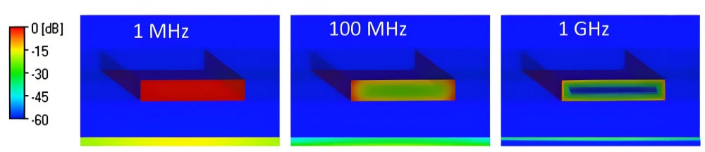
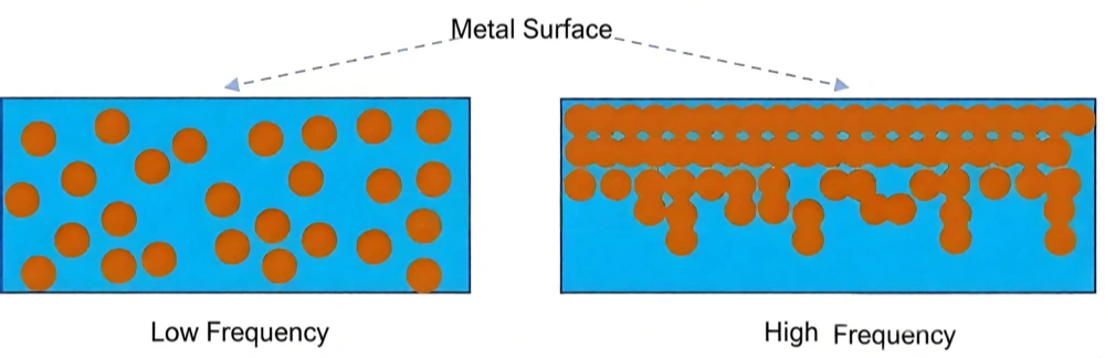
The trend toward high-speed/high-frequency signals makes signal transmission more and more concentrated on the conductor “surface” (called the skin effect). At 1 GHz, the signal transmission thickness on the conductor surface is only 2.1 µm. If the conductor surface roughness is 3–5 µm, signal transmission only happens within the roughness thickness. When the signal frequency goes up to 10 GHz, the transmission thickness on the conductor surface is 0.7 µm. The signal transmission is even more confined within the roughness range. When signals transmit in the roughness range, standing waves and reflections become more and more serious. This makes the signal transmission path longer and increases loss.
Because of the skin effect, if high-speed PCBs keep using standard (STD) copper foil, the result is: as the signal frequency increases, the signal “distortion” caused by the skin effect gets worse. So, low-roughness copper foil is used more and more in current high-speed materials. For example, Mid Loss and Low Loss materials both use reverse treated foil (RTF) as the standard copper foil. Very Low Loss materials also have RTF as standard, but customers mostly use hyper very low profile (HVLP) copper foil in their designs. For Ultra Low Loss materials, HVLP copper foil has become the standard. Scanning electron microscope and metallographic microscope can show the surface morphology of STD, RTF, and HVLP copper foils (0.5 oz thick). STD copper foil matte side roughness (Rz) is about 5 µm, and shiny side roughness is 3 µm. RTF copper foil matte and shiny side roughness is about 3 µm. HVLP copper foil shiny and matte side roughness are both within 2 µm. It is known that copper foil suppliers are also developing NP copper foil with surface roughness below 1 µm. But because of unsolved reliability problems, it is not yet used in actual products.
Improvement of Loss by Low-Roughness Copper Foil
Transmission line loss in PCBs mainly includes dielectric loss and conductor loss. For normal FR4 materials, 1 GHz is the dividing point between dielectric loss and conductor loss. Below 1 GHz, conductor loss is the main part. Above 1 GHz, dielectric loss becomes the main part.
But for Very Low Loss materials, dielectric loss is no longer the main loss. At 10 GHz, conductor loss accounts for about 60% of the total transmission line loss. Figure 4 shows the conductor loss and dielectric loss for microstrip and stripline calculated by simulation based on ITEQ IT-968 material.
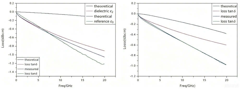
From the figure, the theoretically calculated stripline loss matches the measured loss basically. For both microstrip and stripline, the dielectric loss is much smaller than the conductor loss.
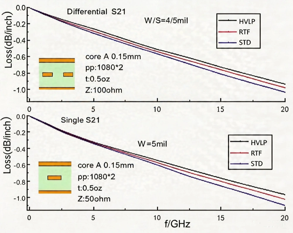
From Mid Loss to Ultra Low Loss materials, the proportion of conductor loss gradually increases. When high-speed materials use different types of copper foil, the measured loss also shows clear differences. Figure 5 shows the stripline signal loss test results for IT-968 material using STD, RTF, and HVLP copper foils.
Processing of Low-Roughness Copper Foil
Although the HVLP copper foil surface is quite smooth, current PCB processes can increase the copper foil surface roughness and affect the performance of HVLP foil. In the inner layer circuit fabrication process, the inner layer must go through dry film pre-treatment and brown oxide process. After these two processes, the Rz roughness of HVLP copper foil increases from about 1.5 µm to around 3 µm. To solve this problem, a matching low-roughness process is available on the market. Compared to traditional brown oxide chemicals, this process does not micro-etch the HVLP copper foil surface. Instead, after cleaning the copper surface, it deposits a tin layer and modifies the surface with siloxane. When laminating with prepreg (PP), the siloxane acts as a bridge. This can increase the bonding strength between the copper foil and PP to some extent.
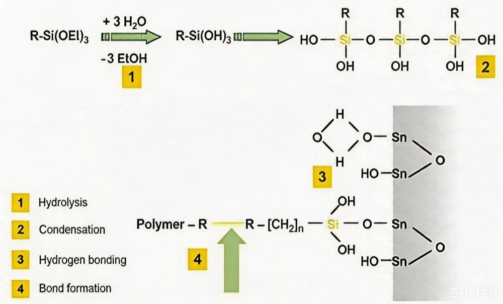
Table 1 compares the surface roughness of HVLP copper foil after using this process and the traditional brown oxide process. From the table, it can be seen that current dry film pre-treatment and brown oxide processes both increase the copper foil surface roughness to some extent. After using the low-roughness process, the copper foil surface roughness is basically the same as the original incoming copper foil.
| Prozess-Typ | Incoming Copper Foil Rz (µm) | After Dry Film Pre-treatment Copper Foil Rz (µm) | After Pre-lamination Treatment Copper Foil Rz (µm) |
|---|---|---|---|
| Traditional Brown Oxide | 1.524 | 2.314 | 3.057 |
| Low-Roughness Process | 1.485 | 1.62 | 1.463 |

