
















1. Via Design in High-Speed PCBs
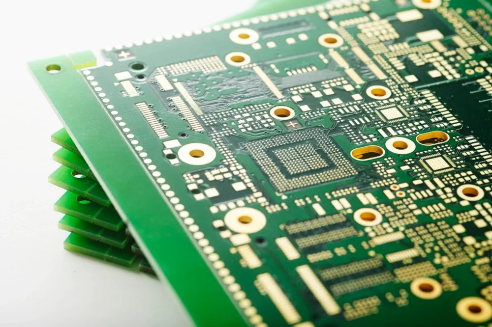
Στο high-speed PCB design, multilayer PCBs are often required. Vias are an important part of multilayer PCB design. A PCB via mainly consists of three parts: the hole, the pad area around the hole, and the POWER layer clearance area. Next, we will discuss the problems and design requirements of vias in high-speed PCBs.
Effects of Vias in High-Speed PCBs
In a high-speed multilayer PCB, when a signal needs to transfer from a trace on one layer to a trace on another layer, vias are required to connect these layers.
When the operating frequency is below 1 GHz, vias can provide good electrical connections, and their parasitic capacitance and inductance can usually be ignored.
However, when the frequency is higher than 1 GHz, the parasitic effects of vias can no longer be ignored because they affect signal integrity. At this time, a via becomes an impedance discontinuity point in the signal transmission path. It may cause signal reflection, delay, attenuation, and other signal integrity problems.
When a signal passes through a via to another layer, the reference layer of the signal trace also becomes the return path for the via signal. The return current flows between reference layers through capacitive coupling, which may cause problems such as ground bounce.
Types of Vias
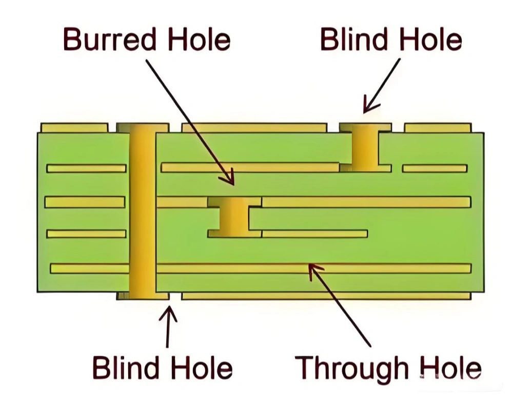
Vias are generally divided into three types:
-
Blind Via
A blind via is a via located on the top or bottom surface of a printed circuit board. It has a certain depth and is used to connect the outer layer traces with the inner layer traces. The depth and diameter of a blind via usually follow a specific aspect ratio requirement. -
Buried Via
A buried via is a connection hole located inside the PCB. It only connects inner layers and does not extend to the surface of the PCB. -
Through Via
A through via passes through the entire PCB. It can be used for internal layer connections or as a mounting and positioning hole for components.
Because through vias are easier to manufacture and have lower costs, they are widely used in general PCB production.
Via Design in High-Speed PCBs
In high-speed PCB design, vias that appear simple can still have a significant negative impact on circuit performance.
To reduce the negative effects caused by via parasitic parameters, the following design methods can be used:
-
Select Proper Via Dimensions
For general-density multilayer PCB designs, a via size of 0.25 mm / 0.51 mm / 0.91 mm (drill hole / pad / POWER clearance area) is recommended.
For high-density PCBs, smaller vias such as 0.20 mm / 0.46 mm / 0.86 mm can be used. Microvias can also be considered.
For power or ground vias, larger via sizes are recommended to reduce impedance. -
Make the POWER Clearance Area as Large as Possible
The POWER clearance area should be large enough. Considering via density on the PCB, it is generally recommended that:
D1 = D2 + 0.41 -
Reduce Layer Changes of Signal Traces
Signal traces should avoid changing layers whenever possible. In other words, the number of vias used for signal routing should be minimized. -
Use a Thinner PCB
A thinner PCB helps reduce the parasitic capacitance and inductance of vias. -
Place Power and Ground Vias Close to Component Pins
Power and ground pins should be connected to vias as close as possible. The trace length between the pin and the via should be minimized because longer traces increase inductance.
At the same time, power and ground traces should be made wider to reduce impedance. -
Add Ground Vias Near Signal Transition Vias
Place several ground vias near signal transition vias to provide a short return path for high-speed signals.
In addition, via length is one of the main factors affecting via inductance.
For vias connecting the top and bottom layers, the via length is equal to the PCB thickness. As PCB layer counts continue to increase, PCB thickness can often exceed 5 mm.
However, in high-speed PCB design, via length is usually controlled within 2.0 mm to reduce signal problems caused by vias.
For vias longer than 2.0 mm, increasing the via diameter can improve impedance continuity to some extent.
When the via length is 1.0 mm or less, the optimal via diameter is usually between 0.20 mm and 0.30 mm.
2. Back Drilling Process in PCB Manufacturing
1. What Is PCB Back Drilling?
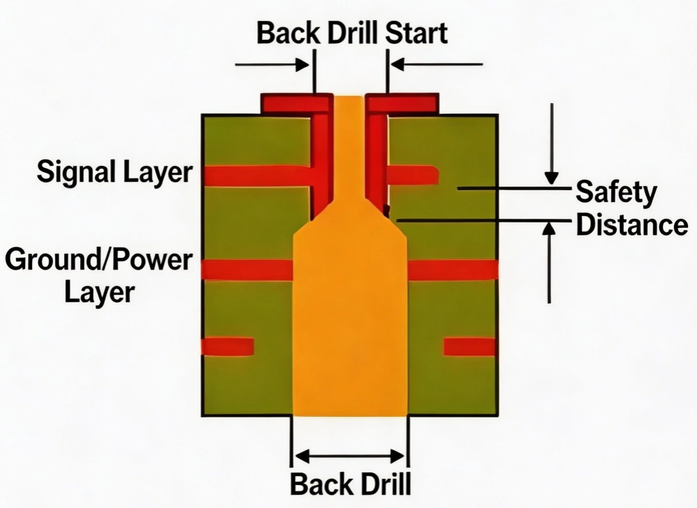
Back drilling is a special type of controlled-depth drilling process.
Στο multilayer PCB manufacturing, for example, when producing a 12-layer PCB, if Layer 1 needs to connect to Layer 9, a normal through-hole drilling process is usually performed first.
After copper plating, Layer 1 is directly connected to Layer 12. However, in this case, only the connection between Layer 1 and Layer 9 is required. Layers 10 to 12 have no electrical connection and become an unnecessary via stub.
This unused section of the via can affect high-speed signal transmission and cause signal integrity problems.
Therefore, this extra via stub (called a stub in the PCB industry) is removed by drilling from the opposite side. This process is called back drilling.
However, the stub cannot be completely removed because some copper remains after the subsequent manufacturing processes, and the drill tip itself has a pointed shape.
Therefore, Κατασκευαστές PCB usually leave a small remaining stub. The remaining stub length is called the B value, which is generally controlled within 50–150 μm.
2. Advantages of Back Drilled Vias
Back drilling provides several benefits:
- Reduces noise interference.
- Improves signal integrity.
- Reduces local PCB thickness.
- Reduces the use of blind and buried vias, lowering PCB manufacturing difficulty.
3. Functions of Back Drilled Vias
The purpose of back drilling is to remove the unused section of through holes that does not provide any electrical connection or signal transmission.
This prevents signal reflection, scattering, and delay during high-speed signal transmission, which can cause signal distortion.
Studies show that, besides PCB design, material selection, transmission lines, connectors, and IC packaging, vias are also one of the important factors affecting signal integrity in high-speed systems.
4. Working Principle of PCB Back Drilling
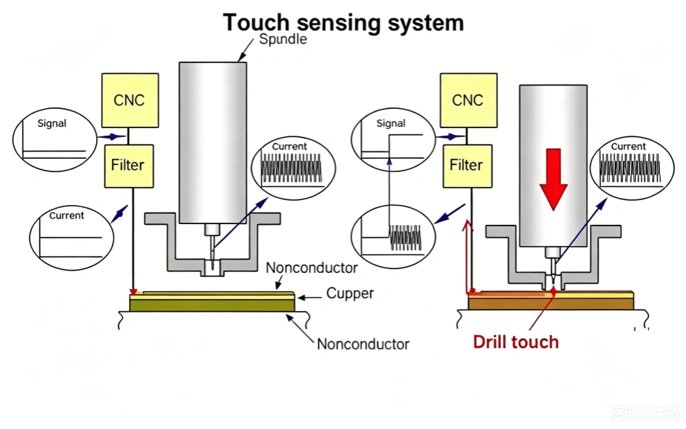
Back drilling relies on the small current generated when the drill bit contacts the copper foil on the PCB surface.
The system detects the PCB surface height position through this electrical signal, then drills according to the preset drilling depth.
When the required drilling depth is reached, the drilling process stops.
5. Back Drilling Manufacturing Process
- Provide the PCB with positioning holes. Use these positioning holes for the first drilling process.
- Electroplate the PCB after the first drilling process. Before electroplating, seal the positioning holes with dry film.
- Create the outer layer circuit pattern on the electroplated PCB.
- Perform pattern plating on the PCB after the outer layer pattern is formed. Before pattern plating, seal the positioning holes with dry film.
- Use the positioning holes from the first drilling process for back drilling alignment. Use a drill bit to perform back drilling on the plated holes that require back drilling.
- After back drilling, clean the PCB with water to remove drilling debris inside the back-drilled holes.
6. How to Handle PCB Holes That Need to Be Drilled from Layer 14 to Layer 12?
1) If there is a signal trace on Layer 11, and through holes are connected to the component side and solder side at both ends of the signal trace, components will be mounted on the component side.
In this case, the signal transmission path is:
Component A → Layer 11 signal trace → Component B
2) According to the signal transmission method described above, the through hole works like a signal trace in this transmission path.
Without back drilling, the signal transmission path will include the unnecessary via section.
3) From the signal transmission path, we can see that the through-hole section from the solder side to Layer 11 does not provide any connection or signal transmission function.
However, this unnecessary via section can cause signal reflection, scattering, and delay.
Therefore, back drilling removes the unused via section to prevent signal distortion caused by reflection, scattering, and delay.
Because drilling depth has manufacturing tolerance requirements and PCB thickness also has tolerance variations, it is impossible to meet the customer’s exact depth requirement 100%.
For back drilling depth control, PCB manufacturers generally follow the principle:
A slightly
shallower depth is better than a deeper depth.
7. Technical Features of Back Drilled PCBs
- Most backplanes are rigid PCBs.
- Layer count is usually between 8 and 50 layers.
- PCB thickness is usually above 2.5 mm.
- Large aspect ratio.
- Large PCB dimensions.
- The minimum first drilling hole diameter is generally ≥ 0.3 mm.
- Outer layer circuits are limited, and press-fit hole array designs are commonly used.
- Back-drilled holes are usually 0.2 mm larger than the holes that need to be removed.
- Back drilling depth tolerance: ±0.05 mm.
- If back drilling is required to reach Layer M, the dielectric thickness between Layer M and Layer M-1 should be at least 0.17 mm.
8. Applications of Back Drilled PCBs
Backplane PCBs are mainly used in:
- Communication equipment
- Large servers
- Medical electronics
- Military systems
- Aerospace applications
Because military and aerospace industries are sensitive fields, backplane PCBs in China are usually supplied by research institutes, R&D centers, or PCB manufacturers with strong experience in military and aerospace projects.
In China, the main demand for backplane PCBs comes from the communication industry. With the rapid development of communication equipment manufacturing, the demand for high-performance backplane PCBs continues to grow.