


In any design work, you will meet many rules and choices. You must think about component placement, routing practice, stackup management, signal and power integrity, and more. You can say that thousands of engineers work to make these processes smooth.
A good place to start is a materials selection guide. A typical PCB has one or more copper layers. These copper layers are laminated between thin, non-conductive substrate layers. The PCB is the physical base that holds electrical parts, conductive traces, pads, and other functional features. In this article, we will look at the materials and design points for each PCB layer: silkscreen, soldermask, copper, and the substrate.
PCB material selection
Handling PCB materials makes any engineer think about heat, mechanical, electrical, and chemical features in the process.
For heat performance, you must think about how hot parts can get and the peak working temperature in the whole design. Mechanical features include the enclosure and form factor, and also density or flexibility, especially for rigid-flex boards.
Electrical properties relate to dielectric needs, such as impedance, signal integrity, and resistance. The design engineer must balance these across the whole board or system. For product life, chemical properties like moisture absorption are needed for humid environments, for example sensors in agricultural IoT. Flammability is also important. In addition, environmental and sustainability limits will affect your PCB material choice.
Key points to check
- Heat: part temperature limits and board hot spots.
- Mechanical: shape, size, density, and flexibility.
- Electrical: dielectric constant (Dk), loss tangent, impedance control, and resistance.
- Chemical: moisture uptake, halogen content, and flammability.
- Environment: RoHS and other rules, recyclability.
Silkscreen
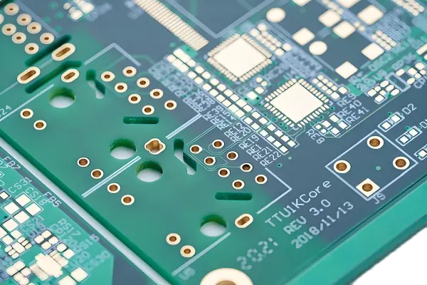
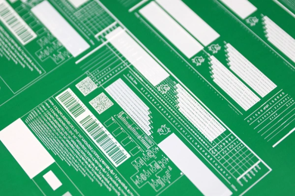
Silkscreen is the layer that prints logos, letters, symbols, numbers, and other info on the board. The name comes from the screen printing method. The main job of silkscreen is to give info for PCB assembly and ID. Polarity, part position, and other details are vital for correct assembly.
The two most common silkscreen print techniques are:
- Liquid Photo Imaging (LPI): a time-consuming, high-resolution print that uses UV-curable ink.
- Direct Legend Printing (DLP): faster and simpler inkjet printing that uses acrylic ink.
From reference marks to applying a UL certification number, a common rule is to use ink that contrasts with the substrate color. White is the most common color, but many other colors are available. It is rare to use more than one silkscreen color on the same board.
Soldermask
The soldermask is the polymer layer over the copper foil that gives the PCB its iconic green look, though other colors are possible. As the name says, it helps prevent solder from moving where it should not go. The soldermask forces solder to land where makers want it, for example on exposed features like annular rings and SMD pads. Soldermask also isolates conductive copper traces so they do not touch solder, metal, or other conductive parts, and it helps prevent oxidation.
Soldermask materials are chosen by how they are applied to the copper layer:
- Epoxy liquid: the cheapest soldermask. It is a thermoset epoxy applied by screen printing.
- Liquid photoimageable soldermask (LPSM): for boards with uneven shapes, this uses a UV-curable ink formula that is coated and then exposed and developed. LPSM may not give a perfect uniform layer, but it covers complex surface features better and can reach into tight spaces near copper traces.
- Dry film photoimageable soldermask (DPSM): for flat boards with uniform topography, dry film is vacuum laminated and then exposed and developed. Dry film gives uniform thickness but can only be used on flat boards.
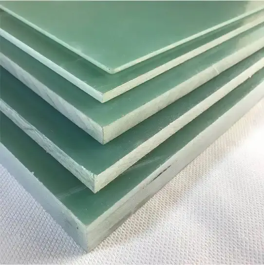
Copper clad laminate (CCL)
Under the soldermask is the copper clad laminate, or CCL. The CCL has two parts:
- Copper foil: a thin layer of conductive copper. Common manufacturing types include STD (E-type, electrodeposited), ANN (E-type, annealed electrodeposited), and AR (W-type, rolled).
- Substrate: the non-conductive layer that gives mechanical strength and support. The substrate is usually made from fr4, which is glass-fiber-reinforced epoxy laminate, and a flame retardant epoxy binder. “fr” stands for flame retardant, and there are many classifications based on performance, combustibility, and the type of reinforcement used.
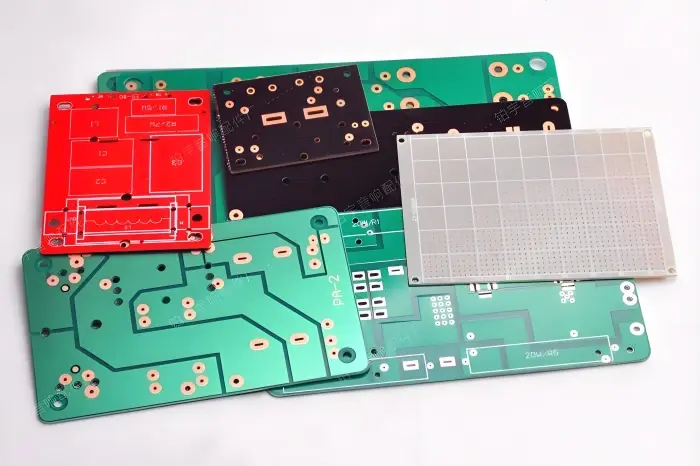
When people say a two-layer or double-sided board, they mean a CCL with copper foil on the top and bottom of the substrate. A standard multilayer board is usually made by stacking two or more double-sided panels with insulating layers between them. That is why most standard multilayer boards come with an even number of copper layers. More layers give you more ground planes to help spread power and lower noise. The only real downside to adding layers is cost.
Why layer count matters
- More layers = more power distribution and better EMI control.
- More layers = higher cost and more complex manufacturing.
- Use more layers when you need controlled impedance, more ground planes, or tight routing.
Future of PCB materials
Small, light boards for mobile devices push demand for more layer stacking and denser designs. Most innovation today is on improving the CCL, not small changes to silkscreen or soldermask.
Enhanced epoxy systems such as Getek, Megtron, 4000-13, and fr-408 perform better than basic fr4 in lowering Dk and loss tangent. High-performance materials like Asahi Glass A-PPE, Nelco 600-21 Si, and Rogers 4350 show clear gains in lower Dk, better impedance control, and reduced jitter for high-speed signals.
Flexible CCL made from polyimide (PI) or polyester give you true flex boards. These are good when you need a bendable circuit.
Strict RoHS rules push for higher heat resistance and reliability. Halogen-free CCL limits chlorine and bromine to 900 ppm or lower. Lead-free CCL replaces the DICY curing system used in standard fr4 with a PN curing system that uses phenolic curing agents so the board works well with lead-free assembly.
Final notes
Choosing PCB materials means tradeoffs. You must match the choice to the product’s use, the signal speed, the manufacturing method, and the environmental rules. Use fr4 for many common boards, but choose high-performance laminates when you need better impedance control or lower loss. For flexible designs, pick PI or polyester based flexible CCL. For assembly, choose the right silkscreen and soldermask method to match the board shape and pad layout.
If you need, I can help turn this into a web page section with headings, short paragraphs, and simple bullets for your foreign site.

