Electronics makers use multilayer printed circuit boards (PCBs) to make circuits take less space. This lets them put more parts on the top side of the board, and it also gives room to run traces on inner layers. Vias are the only way to make electrical links between different layers. Vias are a key part of board design, and they also change how soldering works and can add weak spots. These weak spots can lower the reliability of the whole board. But if designers follow good design rules, they can use vias and still make a reliable PCB.
What a via is?
A via is a hole in a PCB that goes through one or more layers. The maker plates the hole with copper to form a barrel. The ends of the barrel connect to specific traces on the layers. This makes electrical contact between two layers. If a via crosses several inner layers, those inner layers can also connect to the via when the circuit needs it.
There are three main via types: through vias, buried vias, and blind vias.
- Through vias go through the full board thickness. They start at the top layer and end at the bottom layer. Makers can plate or not plate through vias as needed. When a circuit needs it, a plated through via lets other inner layers connect to it.
- Buried vias cross two or more inner layers. They are not visible on the top or bottom. When the circuit needs it, the layers a buried via spans can connect to it.
- Blind vias start at the top layer or the bottom layer and end at an inner layer. On the way they can cross several inner layers and can connect to them when needed.
High density interconnect (HDI) PCBs and flexible PCBs use another via type called microvias. Microvias are very small. Makers drill them with a laser. Each microvia normally goes through one layer only. Makers can stack microvias on top of each other to act like through, blind, or buried vias.
Via size
A via gets stronger and more conductive when its diameter is larger. Larger vias have higher mechanical strength. They also carry more current and move heat better. But using large vias reduces the free area on the board. This can make routing harder when space is tight.
A common practical rule is to use a minimum drill size of 20 mil, an annular ring of 7 mil, and a maximum aspect ratio of 6:1. Here the aspect ratio is board thickness divided by hole diameter. If you keep within these values, the via will be easier to make and will be more reliable for many uses.
Heat and mechanical stress
When a PCB heats up during processing or in use, differences in the coefficient of thermal expansion (CTE) between copper and the laminate can create stress. The laminate structure in the PCB limits expansion in the plane of the board, but the board can shrink or grow more freely through the thickness. This means the vertical direction can see more change.
For example, a fr4 laminate expands or shrinks about four times as fast as copper. So each time the board heats, the copper barrel in the via feels a lot of stress. If the copper barrel is not thick enough, and if the PCB is thick, the board can expand until it breaks the copper. For a 20 mil drill, a 34 mil pad diameter works well. With this pad and a good barrel thickness, a maximum board thickness of 120 mil is a reasonable practice for reliability.
Solder wicking and its effects
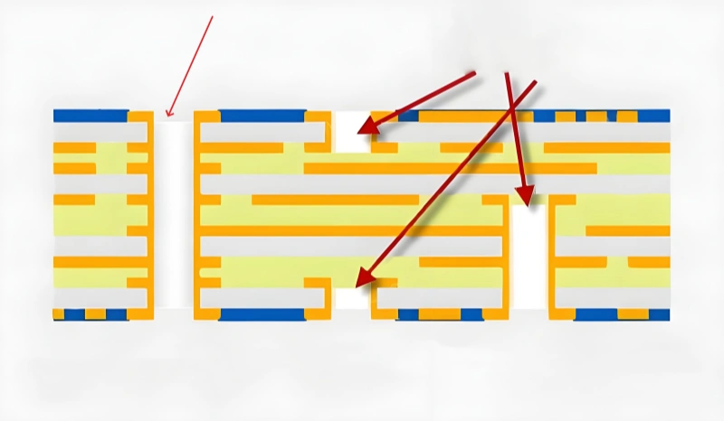
Where you put a via matters as much as its size. Putting a via too close to a pad can cause solder problems. The main issue is solder wicking.
When you heat solder paste on a via and a pad, capillary action draws solder from the pad into the via barrel. The solder moves through the via and collects at the bottom. This leaves the pad with too little solder or no solder at all. A larger via will wick solder faster and more of it. A joint with too little solder can be weak mechanically and have higher electrical resistance.
Here are three common ways to stop solder wicking. Each way can work well.
- Solder mask dam:
Put a solder mask layer between the via and the pad. The mask acts as a barrier and keeps solder out of the via. To fit a mask dam that is wide enough, designers may need to move the via further from the pad. If the board is already dense, or if the board carries high frequency signals, it may not be possible to move the via. - Tenting the via:
If you cannot move the via or add a mask dam, you can tent the via. Tenting means covering the via with solder mask so the via top is fully sealed. Sealing a via fully can stop solder from flowing into it. But it also prevents the via from being used as a test point. Also, contaminants can get into a tented via over time and corrode the copper barrel if the tent is not perfect. - Filling the via:
You can fill a via completely before plating over it. Fill can be conductive or non-conductive. A filled via that is sealed fully gives a better barrier against contaminants. Filling also reduces the risk of solder wicking during assembly. Filled vias are common when you need a flat surface for assembly, for example under BGAs, or when you need better thermal or mechanical performance.
When to use each method
- Use a solder mask dam when you can move the via a bit and the board has room. This is a low-cost fix and works for many boards.
- Use tenting when space is tight and you can accept the via not being a test point. Tenting is lower cost than filling, but it has limits for long term protection against moisture and contamination.
- Use filled vias when you need the best result. Filled vias cost more, but they give a flat top for assembly and keep solder and contaminants out. If you are making many boards or if the board must last a long time in tough conditions, filling is a good choice.
Other reliability factors
Vias can also affect other parts of the design. For example, they can change thermal paths and they can create points where stress concentrates. When a via is near a thermal relief or a heat source, it changes how heat flows in the board. This can affect component life and can change how well a part cools.
Vias near high-speed traces or RF traces can also cause impedance changes. The via barrel and the via pad add capacitance and inductance. Designers must check signal integrity when vias are on critical paths. IDH and microvias help here because they are small and have less impact on high speed signals when placed right.
When building a board for a product that will see many heat cycles, or for a product that must pass strict reliability tests, plan how the vias will behave over time. Use thicker barrel plating when you can. Use stacked or staggered microvias in HDI designs to reduce stress on a single barrel. Use proper pad sizes so the board does not overstress the copper during reflow or during thermal cycling.
For HDI and flexible boards
HDI boards and flexible PCBs use microvias a lot. Microvias are small and have low inductance. This helps with high speed and dense layouts. Each microvia usually reaches only one inner layer. Makers use laser drills to make them. They can stack microvias to connect several layers in a small area. Stacked microvias act like blind or buried vias when you stack them, and they can help keep routing space open on other layers.
For flexible boards, the mechanical flex near vias can hurt the barrel if the via is not placed correctly. In flex areas, try to keep vias out of the main bend lines. Use special via designs and material handling to reduce the risk of cracking when the board bends.
Practical rules and examples
- Minimum drill: 20 mil. This is a common minimum for standard production. Smaller drills need special processes and cost more.
- Annular ring: 7 mil. This gives enough copper around the hole for a reliable connection and for soldering.
- Aspect ratio: limit to 6:1. This keeps plating quality high. If the board is thicker than the recommended value for the hole size, the barrel plating can be thin and can fail.
- Example: if the drill is 20 mil, use a pad diameter of about 34 mil. This gives enough annular ring. For a board up to 120 mil thick, this combination is workable in many factories.
Keep these rules as starting points. Each factory may have slightly different limits. Talk to your board maker early so you can match design choices to what they can do reliably.
Assembly and testing considerations
If you use tenting or fill, think about testing. Tented vias cannot act as probe points. Filled vias that are plated over can still be testable if the fill and top plating are handled correctly during production. If testing is important, plan for test pads, test vias, or other test strategies that fit your assembly process.
When you place a via near a solder pad, plan for the solder process. If you use a lot of vias under a big BGA, consider filling and plating the vias and making the BGA land over a flat surface. This lowers the chance of solder voids and it helps with thermal spreading.
Limpieza y corrosión
Las vías pueden atrapar fundente, humedad y otros contaminantes. Esto se agrava si las vías no son perfectas o si se utilizan como vías térmicas que permiten la entrada y salida de humedad durante los ciclos térmicos. Realice una buena limpieza tras el montaje cuando el diseño lo necesite. Utilice materiales y acabados fiables que resistan la corrosión en el entorno previsto. Las vías rellenas ayudan a evitar la entrada de contaminantes.
Conclusión
Las vías son necesarias en las placas de circuito impreso multicapa. Permiten colocar más piezas y enrutar redes complejas. Pero las vías también modifican el comportamiento de la soldadura y añaden puntos de tensión mecánica y térmica. Estos riesgos pueden reducirse con unas buenas normas de diseño y tomando las decisiones adecuadas al principio del proyecto.
Los diseñadores deben estudiar la fiabilidad desde el principio. Un estudio de fiabilidad aumenta las posibilidades de éxito, reduce los costes a lo largo de la vida del producto, acorta el tiempo de comercialización y mejora la satisfacción del cliente. Para hacer un buen diseño de fiabilidad se necesitan las personas adecuadas, las herramientas adecuadas y tiempo suficiente. Planifique los tipos, tamaños, ubicación y tratamiento de las vías con el fabricante y la empresa de montaje. Utilice diques de máscara de soldadura, tenting o rellenado de vías cuando cada método sea adecuado. Utilice microvías para diseños HDI y flexibles cuando sea necesario.