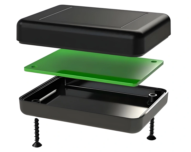
Printed circuit board design is an important factor that affects the performance of many electronic products. Making a reliable product and then winning market success is the biggest reward for careful thinking on every design issue. Choosing the right board-level shielding cavity is only one part of a successful design. Other key issues must also be considered carefully, such as the working environment, the total number of products to be made, the mounting method to be used, the test and inspection methods planned, and the layout of the PCB and components.
Just like power supply selection, the choice to use an RF shielding cavity is often made at the end of the design process. This often leaves too little space for the shielding cavity. As a result, the cavity may affect other parts of the design in terms of physical structure.
3DS — Design, Development, Drafting
The design and development of PCB board-level shielding cavities and systems can be divided into three key steps: design, development, and drafting. Active communication and consultation between the cavity user and the cavity design team are very important. It is best to find a cavity manufacturer that can provide initial design guidance, advice on use, site visits, prototype design, sample production, coating and thickness selection, processing, assembly, and cost-saving review.
To get market profit from a product, cost must be controlled. Structural design, together with a detailed design plan and customer input, may help achieve the ideal goal: getting the needed result with limited cost.
Form Selection
When choosing the form of the cavity, many factors must be considered. What exactly needs to be shielded? What is the exact nature of the interference source? After the cavity is mounted on the PCB, will the customer still need to open it for changes, testing, inspection, or adjustment? Is the cavity mounted by through-hole methods or surface mount methods? What is the expected production volume? Does this volume match the cost of machine placement? Which circuit areas need shielding, or need to be separated from other areas? Should this application use one cavity or several cavities? Will the final product go through impact testing, vibration testing, or drop testing in packaging?
Shielding Forms
For a specific application, careful review of the questions above helps choose the most proper and most economical shielding form. Different four-sided shielding cavities can be selected for different applications.
A four-sided shielding cavity with finger spring cover has a fence on all four sides. The fence and the series of pins at the PCB edge can be soldered to the PCB by hand soldering, wave soldering, or through-hole reflow soldering. Finger spring covers are often used for this type of cavity. If the fence height is enough to hold the finger spring, then the finger spring cover is the best choice among removable covers. Finger spring sizes, such as standard height or low profile, can be made as needed. If there is not enough space outside the fence for external finger springs, then internal finger springs should be chosen. Also, if the external finger springs and internal finger springs have the same shape on opposite sides, they can be used in a mixed way.
A surface-mount four-sided cavity with finger springs is another shielding cavity option. This type of cavity is the same as a normal four-sided cavity, except that it does not have fixed pins. It is often soldered to the PCB along a continuous line by seam soldering. When judging the relation between fence height and finger length, the designer must include the thickness of the solder fillet at the bottom of the fence.
Another way to replace a continuous seam-soldered fence is to make the fence along the PCB edge with gaps. This method reduces the amount of solder used to attach the fence to the PCB. It also leaves space for traces to pass through the fence boundary, without needing special trace clearance vias or a multilayer PCB. If machine placement is used to mount the fence on the PCB, surface mount technology must be used. This may require the use of stamped fence structures, as shown in Figure 1.
A four-sided PCB cavity can also use a flat fold-over lid, as shown in Figure 2. This type of lid has lower production cost, especially during the development stage. The only weakness of this design is that it cannot fully guarantee a good connection between the lid and the fence, except where the lid-retaining strips are used. Any gap in the connection will affect the EMC performance of the cavity. These lid-retaining strips can be either folded type or wrapped type, as shown in Figure 2 and Figure 3. Both types of strips can support the lid for moving and replacing more than five times.
Flat Fold-Over Lid
When the real application needs a low-profile fence and lid, a snap-on lid can be used. Small tabs on the side wall of the lid fit into small slots on the side wall of the fence. This design can reduce fence height to 1.5 mm. Like the lid-retaining strip and gap lid, this design also cannot fully guarantee a good connection between the fence and the lid, unless the tabs are fixed firmly in place. Also, the more tabs there are on the wall, the harder it becomes to remove the lid when repair or adjustment is needed after installation.
Some designers prefer to use placement equipment from a surface mount line to make the lid and the fence into one unit. In this case, the lid is only opened when components inside the cavity need to be reworked. Choosing this design means that small arrays of holes must be left on the lid so that heat can enter the cavity and solder the internal electronic parts onto the PCB, as shown in Figure 4. Unfortunately, these holes will reduce the shielding performance of the cavity by about 20 dB.
When cavity installation is done after testing, or when PCB output volume is very high, choosing a five-sided cavity is more cost-effective. This choice can be made by solder pins, spot-weld corners, butt-weld corners, or thermal reflow holes. So far, the lowest-cost way to develop five-sided cavities and make small-volume production is to use formed five-sided cavities. As shown in Figure 5, these are made by marking on a flat sheet. When they are installed on the PCB, the user only needs to fold them into the needed shape.
Shielding Materials
For most RF shielding, almost any base material, such as copper, brass, stainless steel, aluminum, or nickel silver, can be used to make the shielding enclosure. In the mounting process for soldering components to the PCB, plating is used more often than nickel silver. Bright tin plating was used in the past. However, with the use of the RoHS rules on harmful substances, PCB production lines switched to lead-free soldering. The reflow temperature of lead-free solder is equal to or even higher than the melting point of bright tin. Because of this, the use of nickel silver also changed. Of course, silver plating or gold plating can also be used, but the cost is clearly too high.
At low frequency, interference is usually caused by magnetic fields. Although thicker steel sheets or phosphor bronze are sometimes used to make shielding cavities, special materials such as Mu-metal or RF materials are used more often.
The frequency limit for making shielding cavities with metal foil is usually around 3 to 5 GHz. If the frequency goes beyond this range, two effects will limit the shielding effectiveness or reduce its function. Because of the distributed capacitance between the cavity and the electronic components on the PCB, any small movement in the cavity metal can create a microphonic effect. In this frequency range, solid processed structures are usually chosen for shielding, so these effects can be avoided.
Another high-frequency effect may happen at the harmonic frequency of the circuit operating frequency, where the cavity space becomes part of a waveguide. In this case, the cavity may behave more like a resonant cavity than a shield. This effect can be avoided by adding absorbing material inside the cavity or by carefully choosing the cavity size.
Production and Assembly Design
A key factor in cavity design is knowing the production volume of the final component or product. This decision will determine the final production method and, to some extent, the choice of shielding form. As discussed above for fence-lid designs and five-sided cavities, it is clear that making one complete unit is much cheaper than joining two parts together to form the shield.
The chosen production method also affects component cost. For example, compare the cost of photochemical machining, or PCM, with stamping, or with a mixed method that uses both. Will the components be placed by hand or by machine? If machine placement is used, most machines pick up parts with a vacuum nozzle, so placement targets are needed. Some machines use a clamp-type system to grab parts, but this type of machine is not very common.
For machine placement, the coplanarity requirement of the PCB edge fence should be within 0.1 mm to make sure the cavity is on the solder paste during placement or when entering the reflow oven.
Common Shield Materials for Machine Processing
For most RF shielding, almost any base material, such as copper, brass, stainless steel, aluminum, or nickel silver, can be used to make the shield. In the mounting process for soldering components to the PCB, plating is used more often than nickel silver. Bright tin plating was used in the past. However, with the use of the RoHS rules on harmful substances, PCB production lines switched to lead-free soldering. The reflow temperature of lead-free solder is equal to or even higher than the melting point of bright tin. Because of this, the use of nickel silver also changed. Of course, silver plating or gold plating can also be used, but the cost is clearly too high. At low frequency, interference is usually caused by magnetic fields. Although thicker steel sheets or phosphor bronze are sometimes used to make shielding cavities, special materials such as Mu-metal or RF materials are used more often.
The frequency limit for making shielding cavities with metal foil is usually around 3 to 5 GHz. If the frequency goes beyond this range, two effects will limit the shielding effectiveness or reduce its function. Because of the distributed capacitance between the cavity and the electronic components on the PCB, any small movement in the cavity metal can create a microphonic effect. In this frequency range, solid processed structures are usually chosen for shielding, so these effects can be avoided.
Another high-frequency effect may happen at the harmonic frequency of the circuit operating frequency, where the cavity space becomes part of a waveguide. In this case, the cavity may behave more like a resonant cavity than a shield. This effect can be avoided by adding absorbing material inside the cavity or by carefully choosing the cavity size.
Final Notes
For most RF shielding applications, the key is not only choosing the right shield shape, but also matching the right material, process, and assembly method. A good design should balance shielding effect, cost, production volume, and later rework needs. In real PCB projects, the best solution is often not the most complex one. It is the one that can be made, assembled, tested, and repaired in a stable and low-cost way.
1. What is PCB shielding and why is it important?
PCB shielding is used to block electromagnetic interference (EMI). It helps improve signal stability and ensures reliable product performance.
2. What types of PCB shielding cavities are available?
Common types include four-sided shielding cans, surface-mount shields, snap-on lids, and five-sided cavities. Each type fits different design and cost needs.
3. How do I choose the right shielding cavity for my PCB?
You should consider interference source, space, production volume, mounting method, and whether the shield needs to be removable for testing.
4. What materials are used for RF shielding in PCB?
Common materials include copper, brass, stainless steel, aluminum, and nickel silver. Special materials like Mu-metal are used for low-frequency magnetic shielding.
5. Does shielding design affect PCB cost?
Yes. The shielding structure, material, and assembly method all affect cost. A simple integrated design is usually more cost-effective.
6. What is the difference between surface mount and through hole shielding?
Surface mount shielding is easier for automated assembly. Through hole shielding offers stronger mechanical support but may increase cost.
7. How can I improve EMI performance in PCB design?
You can improve EMI performance by using proper shielding, optimizing layout, reducing noise sources, and choosing the right materials and grounding methods.
8. Can shielding cavities be reused or removed?
Yes. Some designs like finger spring covers allow easy removal for testing, repair, or adjustment.

