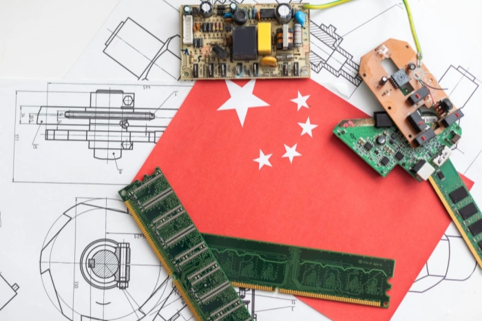
Since the European Union formally legislated “lead-free” in December 2003, the global electronics industry felt a strong impact. By July 2006, the EU directives on Waste Electrical and Electronic Equipment (WEEE) and on the Restriction of Hazardous Substances (RoHS) came into force. At the same time, lead-free and halogen-free rules from the Japan Electronics and Information Technology Industries Association (JEITA) and the U.S. National Electrical Manufacturers Association (NEMA) for the electronic packaging industry also took effect. From then on, electronic products placed on the market must not contain lead, mercury, cadmium, hexavalent chromium, or restricted amounts of polybrominated biphenyls (PBB) or polybrominated diphenyl ethers (PBDE) and other harmful substances. This change affects the global supply chain and the development of related industries, including the PCB sector. This article explains, across raw material control, selection and control of lead-free processes, and SMT final assembly, how next-generation PCB products can meet increasingly strict environmental rules.
1. Selection and control of raw materials
It is well known that mercury, cadmium, and hexavalent chromium are almost never used in the PCB industry. Apart from trace amounts in wet processing, PCB makers do not deliberately use these elements. So, when choosing raw materials and processes, keeping lead (Pb) and halogen levels under limits is the main requirement to meet basic environmental rules. For PCB surface metal finishes, the goal is to be lead-free (below 0.1% Pb). Traditional PCB and SMT industries used a lot of lead–tin alloys, such as HASL and solder paste. Lead is a heavy metal element and it exists widely in nature. When human lead intake exceeds safe levels, symptoms like anemia, calcium deficiency, and reduced immunity can appear.
1.1 Why use lead-free solder?
Harm from lead in solder: Even though the lead contained in solder is a small share of total lead use in some scales, it can spread and is hard to fully recover. Environmental pollution and worries about lead poisoning push the move away from lead. In PCBs, halogens (fluorine F, chlorine Cl, bromine Br, iodine I) are mainly used in laminates and inks.
1.2 Material screening
A finished PCB mainly contains three groups of things: the laminate (base material), the metal surface finish layers, and inks.
1.2.1 Base material
Common laminates such as افآر-۴ and CEM-3 often contain a lot of brominated epoxy resins. These resins can include tetrabromobisphenol A, polybrominated biphenyls, and polybrominated diphenyl ethers. When these materials burn, they can release highly toxic compounds like dioxins (TCDD) and furans. If humans ingest such compounds, they are hard to remove from the body and they pose serious health risks. Therefore, the copper-clad laminate industry must move to halogen-free base materials. Halogen-free means chlorine and bromine are both below about 0.09%. Use phosphorus-containing epoxy resins to replace brominated epoxy resins. Use nitrogen-containing phenolic resins to replace traditional dicyandiamide curing agents.
Also, eco-friendly laminates must have strong heat resistance. They must withstand multiple lead-free SMT reflow cycles around 260 °C without discoloring, delaminating, deforming, or warping.
1.2.2 Surface metal layers
The industry now widely uses lead-free HASL with a tin–silver–copper formula (for example, 95.5Sn–3.9Ag–0.6Cu) instead of lead–tin alloys. Lead-free PCB surface coatings must show good wetting and flow. They must produce low thermal stress and resist oxidation at high temperature. This helps lead-free SMT processing. The flux used for HASL must also be eco-friendly, recyclable, and compatible with SMT fluxes so they reflow together.
1.2.3 Inks
Inks left on the PCB include solder mask inks, legend inks, and via-fill inks. Ink formulas are similar to laminate formulas. They mainly contain resin, brominated flame retardants, and curing agents. Many modern ink brands already produce inks without harmful substances. The choice of ink must meet environmental rules and also survive repeated high-temperature lead-free SMT cycles. Inks must not delaminate, discolor, flake, or crack after processing.
1.2.4 Control of lead-free materials
Raw material management is a very important link for eco-friendly PCB production. For example, if a leaded solder bar is mistakenly added to a pure tin pot, the result can be catastrophic. Residues from indirect materials like flux must not be ignored. Practical measures include:
Set up material codes for halogen-free and lead-free raw materials.
Use color marks and print an approved “green” label on outer and inner packaging.
Store eco-friendly materials separately in the warehouse and on the production floor. Assign specific staff to add them in production.
Implement a “green qualified supplier” certification program.
2. Selection and control of lead-free processes
Lead-free surface processes for PCB include electroplated Ni/Au, electroless Ni/immersion Au, OSP (organic solderability preservative), immersion tin (chemical tin), and immersion silver (chemical silver).
2.1 Steps to introduce lead-free processes
Follow these steps: engineering design → technical development → reliability evaluation → material procurement → project implementation and technical rollout.
2.2 Process implementation and control
2.2.1 Engineering CAM design
Project-level design for eco-friendly PCBs must consider effects on SMT post-processing and PCB function after assembly. CAM work should account for SMT steps.
Example layout design (routing and pad shapes):
Prevent component movement during wave or selective solder. Make some pad diameters a little smaller to reduce the risk of bridging.
Prevent QFP lead bridging during wave solder. If needed, tilt QFP parts and design dummy solder areas.
For soft-melt chips, keep earlier rules. Place protective film openings near inner edges.
Prevent board warpage:
Check the board’s heat resistance. Pay attention to soft-melt peak temperatures under moisture.
For large boards or boards that carry heavy parts, prepare support areas in the center to reduce warping.
When placing parts, try to make thermal mass distribution even.
Thin multi-layer boards or boards with cut grooves are easy to warp under soft-melt heat. Consider shape and size carefully.
2.2.2 Technical development
Process development and control is a key area for eco-friendly PCB production. Practical actions include:
Do not run eco-friendly and non-eco-friendly materials on the same line. Separate processes like developing and final cleaning.
Mark eco-products on MI (manufacturing instruction) sheets. Require a signature confirming the lead-free process to remind operators.
Make eco-product production tools and fixtures obvious with visible labels.
Inks must withstand repeated high-temperature lead-free SMT. Pre-treatment and substrate drying are very important. After HASL or lead-free SMT, ink may peel at hole edges. This often comes from moisture left in holes and on surfaces. Under high heat, moisture expands and separates ink from copper.
Do not add thinners to solder mask ink. This avoids fast solvent evaporation in holes under high heat, which can cause hole damage.
Keep copper content in HASL solder pots below 0.85%.
2.2.3 Reliability evaluation
Compared to non-eco PCBs, eco-friendly PCBs need stronger reliability tests. Add these tests:
Solderability test. Use the same type of lead-free solder that production will use.
Thermal shock test. Conditions: -40 °C / 85 °C / 125 °C. After 3000 cycles there should be no cracks.
Thermal cycling test. No cracks and no shrinkage voids.
Damp heat test. Conditions: 60 °C and 90–95% RH for 500 hours. Under long-term high temperature and humidity, there should be no metal-whisker-like products.
3. Eco-friendly PCB in SMT final assembly
3.1 Lead-free SMT characteristics
Lead-free solder has a higher melting point. It shows lower wetting and flow, higher thermal stress, poorer wettability, and is more prone to oxidation. This requires stricter manufacturing conditions and quality control.
3.1.1 SMT line design
Increase preheat temperature. Control the SMT line speed to about 1.2–1.8 m/min. Set the conveyor tilt to 3–5 degrees. Provide thermal compensation where needed so the SMT area stays at a stable temperature.
To ensure good wetting, keep the proper preheat temperature range.
Solder pot and thermal control:
The part surface temperature on the board must stay below its guaranteed thermal limit while the board back side may reach about 250 °C. Shorten distance between heating stages to keep the temperature drop between waves within about 55 °C.
When using Sn–Ag–Cu solder, it may be possible to stop using the first wave.
3.1.2 Manual rework soldering
Set soldering iron temperature to about 370 ± 10 °C. Use a chrome-plated tip. Use an 80 W iron for short contact times like 3 seconds. Preheat the substrate to 50–60 °C. If a soldering iron is unused for a long time, clean contaminants from the tip. Wet the tip with fresh solder, then switch off power to prevent oxidation.
3.1.3 Using nitrogen protection and its benefits
Improve the process atmosphere.
Reduce oxidation and improve solder wetting on component leads.
Improve appearance, as lead-free joints are less shiny.
Reduce color change caused by long high-temperature exposure in lead-free processes.
3.2 Research and special process notes
3.2.1 Study low-melting-point solders below 125 °C as an option for special cases.
3.2.2 Use local heating methods (spot heating, infrared, or RF) to solder certain parts at 240–260 °C. Parts must tolerate heat for more than 40 seconds. Local heating tools may include lasers, xenon flash (non-contact), hot sliders, or pulse heaters (contact).
3.2.3 Follow standards like ISO 14000 and customer process specs. Green practices include lead-free and halogen-free materials, air purification, and flux recovery systems that can filter and recycle about 90% of flux.
3.2.4 Use anti-mildew and anti-termite measures where needed for PCBs.
3.2.5 Research and apply recyclable and biodegradable organic PCB substrates.
4. Summary checklist for engineers and production teams
Verify all raw material certificates of analysis (COA). Confirm halogen and lead levels are below limits. Keep COA files for audits.
Use separate storage and clear labeling for lead-free and halogen-free materials. Train staff to avoid cross-contamination.
Update CAD and CAM rules for lead-free processing. Adjust pad sizes and solder mask openings as needed.
Conduct trial runs and evaluate solderability, thermal shock, thermal cycling, and damp heat tests. Track results and compare to baseline.
Control HASL bath composition and monitor copper content. Keep plating and cleaning processes well controlled.
Ensure preheating zones on SMT lines are stable. Use nitrogen when possible to reduce oxidation.
Improve drying and bake-out steps to remove moisture before high-temperature processes. Use controlled ovens for substrate drying.
Apply conformal coating when product use or environment requires extra moisture protection.
Maintain supplier audits and approve only green qualified suppliers. Require supplier declarations for RoHS and halogen-free status.
Plan for end-of-life recycling. Design for disassembly and material recovery when possible.
5. Final notes
Meeting RoHS rules is not just a material change. It is a change across the whole supply chain. It affects material selection, factory process control, product design, and final assembly. It also changes testing and long-term reliability work. Teams must plan carefully and act in steps. Start with strict material control and CAM design. Develop stable lead-free processes. Run thorough reliability tests. Train operators and keep clear records. With these steps, PCB makers can deliver RoHS-compliant and reliable products for customers and for the environment.