PCB designFR-4 PCB Guide: Properties, Limits & Material Choices Leave a Comment | Styczyń 19, 2026 | PCB design | 5 minutes of reading FR-4 PCB Guide: Properties, Limits & Material Choices Read Post »
UncategorizedPCB Thermal Management — Cooling and Heat Design Leave a Comment | Styczyń 19, 2026 | Uncategorized | 6 minutes of reading PCB Thermal Management — Cooling and Heat Design Read Post »
PCB design PCB manufacturersAluminum Substrate PCB Guide: Thermal Design & LED Uses Leave a Comment | Styczyń 16, 2026 | PCB design, PCB manufacturers | 9 minutes of reading Aluminum Substrate PCB Guide: Thermal Design & LED Uses Read Post »
PCB design PCB manufacturersFPC Flex Circuit Stiffening and Reinforcement Processes Leave a Comment | Styczyń 16, 2026 | PCB design, PCB manufacturers | 7 minutes of reading FPC Flex Circuit Stiffening and Reinforcement Processes Read Post »
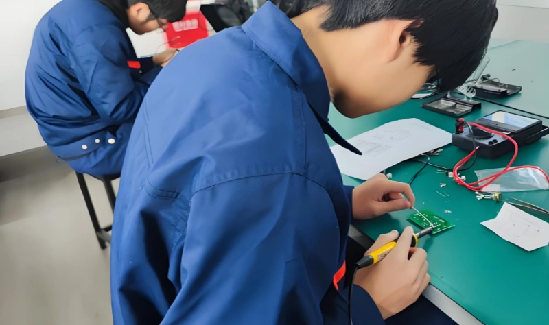
UncategorizedPCBA Manual Soldering Best Practices Leave a Comment | Styczyń 15, 2026 | Uncategorized | 7 minutes of reading PCBA Manual Soldering Best Practices Read Post »
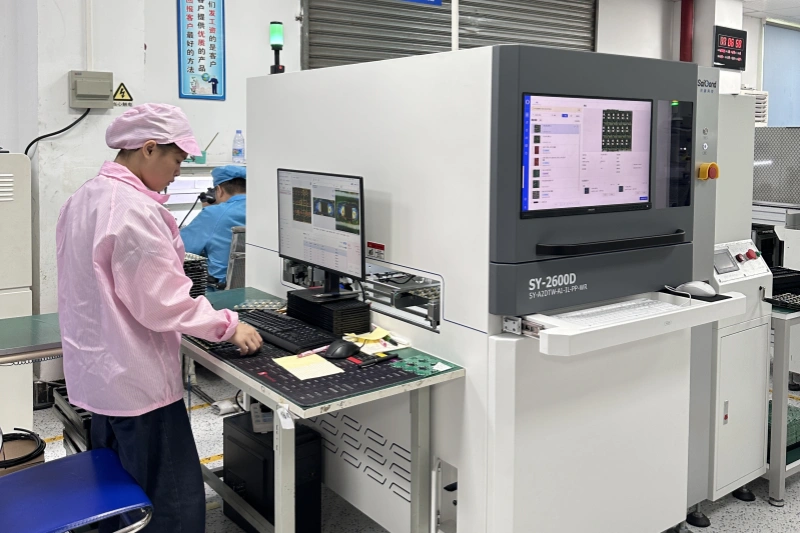
PCB manufacturersPCB Production Quality Control: Challenges, Practices, and Philifast’s Solutions Leave a Comment | Styczyń 14, 2026 | PCB manufacturers | 7 minutes of reading PCB Production Quality Control: Challenges, Practices, and Philifast’s Solutions Read Post »
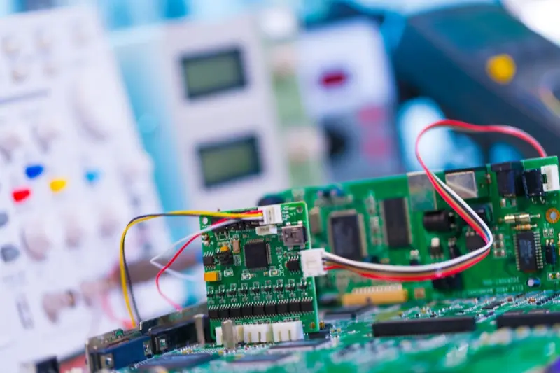
PCBA PCB design PCB manufacturersPCB Design: DFT, DFM, DFA — Key Design Considerations Leave a Comment | Styczyń 13, 2026 | PCBA, PCB design, PCB manufacturers | 7 minutes of reading PCB Design: DFT, DFM, DFA — Key Design Considerations Read Post »
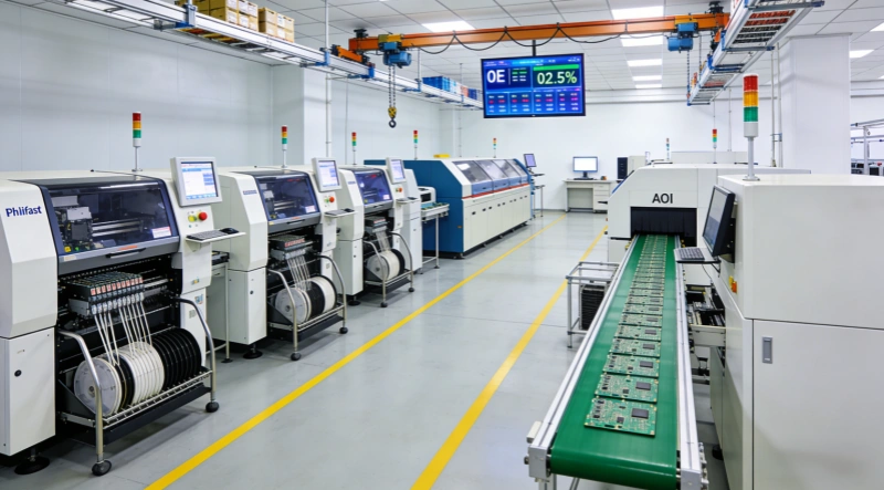
PCB design PCB manufacturersWhat is Philifast’s SMT Production Line Process? Leave a Comment | Styczyń 9, 2026 | PCB design, PCB manufacturers | 8 minutes of reading What is Philifast’s SMT Production Line Process? Read Post »
UncategorizedThermal Design of LED Aluminum PCBs Leave a Comment | Grudziyń 26, 2025 | Uncategorized | 10 minutes of reading Thermal Design of LED Aluminum PCBs Read Post »
UncategorizedComplete PCB Design Workflow: From Schematic to Gerber Files Leave a Comment | Grudziyń 25, 2025 | Uncategorized | 14 minutes of reading Complete PCB Design Workflow: From Schematic to Gerber Files Read Post »