
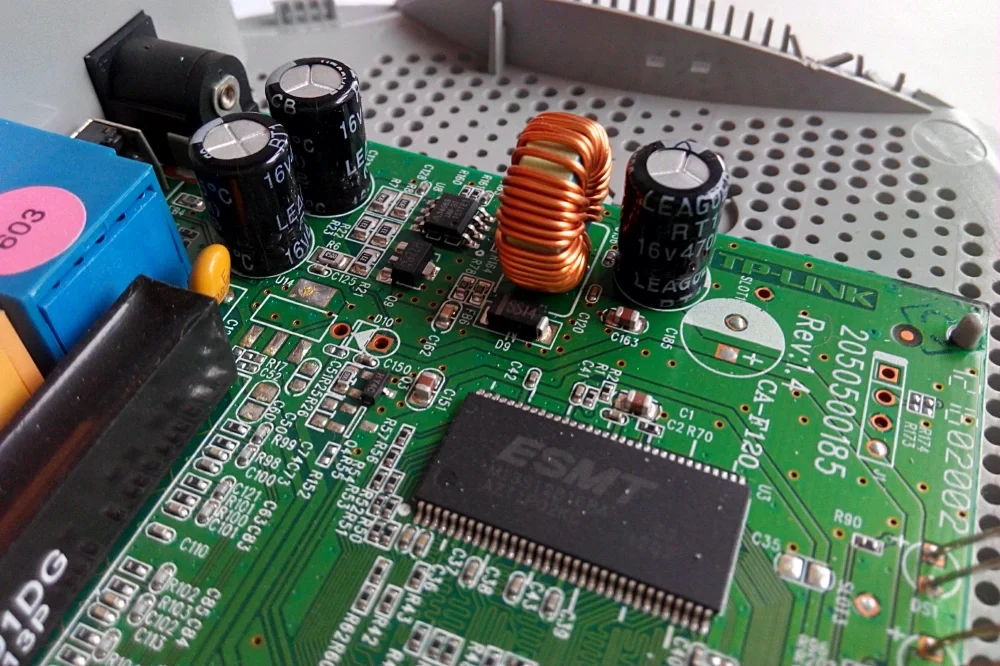
What is inductance?
Inductance is the numerical integration of the surface magnetic field strength.
Closed magnetic flux lines form around a current. Their direction follows the right-hand rule.
Inductance is the number of magnetic flux line turns around a conductor when the current is 1 A. Inductance relates to the number of flux line turns around the conductor per unit ampere of current.
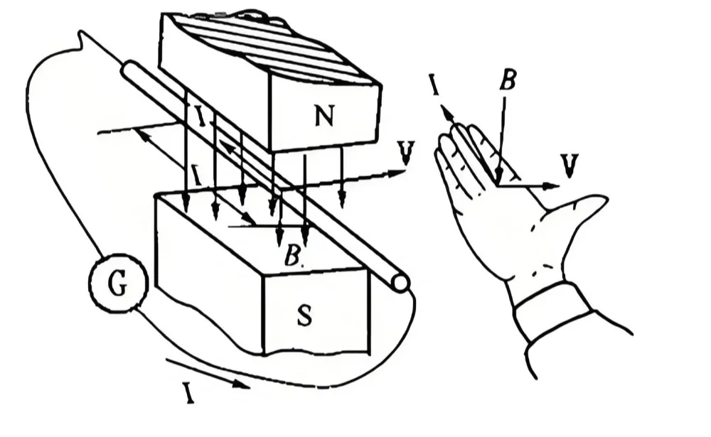
To tell apart the source of the magnetic flux lines, inductance is usually divided into self-inductance and mutual inductance. To know the size of the current loop that the flux lines surround, loop inductance and partial inductance are introduced.
Classification of inductance
Using the right qualifiers helps you understand and remember inductance. It also stops you from using the wrong terms and causing confusion.
The number of magnetic flux line turns around a conductor when a unit ampere current flows is called inductance.
When a unit ampere current flows through a conductor, the magnetic flux line turns around that conductor is called the self-inductance of the wire. The self-inductance of a wire has nothing to do with the currents in other wires. The number of flux line turns from its own current does not change.
When a conductor carries a unit ampere current, some of its magnetic flux lines surround another conductor. This number of flux line turns is the mutual inductance. Mutual inductance is mutual: some of my flux lines surround you, and the same number of your flux lines surround me. Mutual inductance is affected by the distance between the two wires. When they get closer, mutual inductance increases. When they move apart, it decreases.
Self-inductance plus the effect of mutual inductance gives the effective inductance. The effect of mutual inductance is different for different current directions.
If the currents in two adjacent wires A and B flow in the same direction, effective inductance = mutual inductance + self-inductance.
If the currents in A and B flow in opposite directions, effective inductance = mutual inductance – self-inductance.
Mutual inductance and crosstalk
A signal on a transmission line is basically an alternating electromagnetic field. Because of mutual inductance between lines, when the magnetic field changes, it creates an induced voltage on the other wire.
The induced voltage from inductive coupling and the induced current from capacitive coupling together form crosstalk.
Because both the induced voltage and induced current depend on conductor spacing and the speed of voltage change, the main factors that affect crosstalk are wire spacing and signal frequency. So to keep the system running at high speed, we increase the spacing between two transmission lines. This reduces mutual inductance and mutual capacitance, and then reduces crosstalk.
Transmission line spacing design: 3H/W rule
What is the right transmission line spacing?
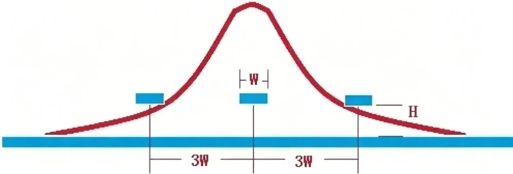
When current flows in a transmission line, the electromagnetic field energy distribution is like a normal distribution. About 70% of the energy is within 3H around the wire. If the distance between two wires is greater than 3H, the mutual inductance between them drops sharply. This can reduce crosstalk a lot. This is the origin of the 3H/W rule of thumb for PCB design engineers.
According to the rule of thumb, with a 3W spacing, near-end crosstalk is about 1.9%, and far-end crosstalk is about -2.2% (only for microstrip lines; striplines have almost no far-end crosstalk. This is why we suggest routing high-speed transmission lines on inner layers).
H is the height from the trace to the reference plane. For a common 50-ohm impedance line, the line width W is close to H. For easier measurement, W is often used to express it. In real design, W is usually larger than H.
Also, reducing H strengthens coupling to the GND plane, so energy is concentrated in a smaller area. With the same spacing, crosstalk is smaller. Because H is smaller, the impedance line width also becomes smaller. This increases the spacing without needing extra space, and again reduces crosstalk. Did you get this skill?
Effect of inductive discontinuity on signals and capacitive compensation
If there is an inductive discontinuity in the middle of a transmission line, how does it affect the signal? Xiao Chen imagined: Because of the extra L in the line, according to the impedance formula, the transient impedance becomes larger. So the signal reflects at that point.
How can I improve it? I had another idea: Since you added inductance, I will counter it with capacitance. I will add capacitive compensation at the place where inductance changes, increase capacitance to balance impedance again and remove the reflection. Is this what really happens? Let’s check.
I built a 50-ohm transmission line link in software and added termination. The source is 1 GHz, with 2V source voltage. Through voltage division, the voltage on the transmission line is 1V. With full reflection at the end, the transient voltage is 2V. I simulated an inductive discontinuity in the middle of the line. I observed the waveform when the signal reaches the end. I also tried capacitive compensation to see if it can remove the effect of the inductive discontinuity.
C = L / (Z²) = 8 / (50 * 50) = 3.2 pF
For better compensation, it is split into two 1.6 pF capacitors in parallel.
Signal waveform before capacitive compensation
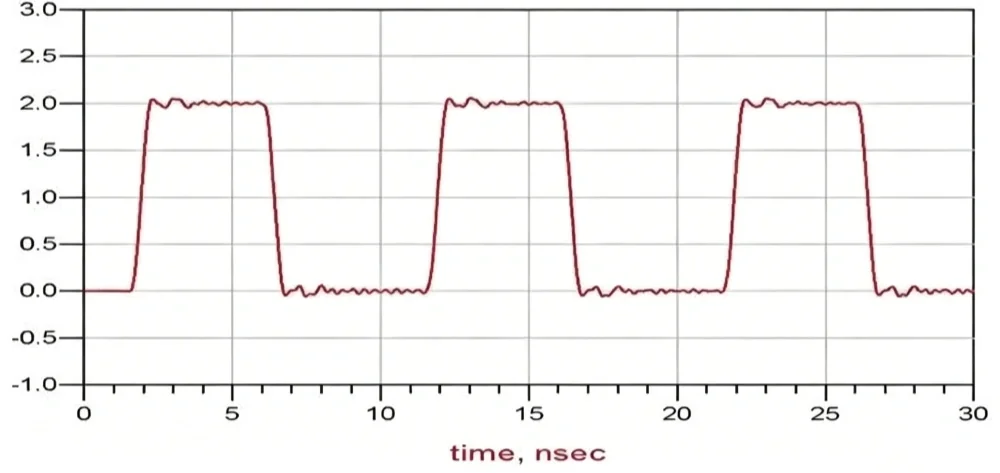
From the simulation waveform, we can see that because of the 8 nH inductive discontinuity in the middle, the reflection causes overshoot. The overshoot is about 300 mV.
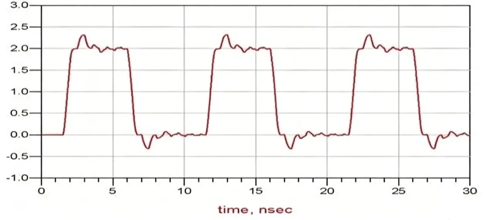
Signal waveform after capacitive compensation
From the simulation waveform, we can see the overshoot is basically gone. Only some tens-of-mV glitches remain. By adding local capacitive compensation, we increase the local capacitance. According to the impedance formula, when capacitance goes up, impedance goes down. This cancels the effect of high inductance on impedance, making impedance balanced. It removes or reduces reflection, and the signal overshoot disappears.
In real design, adding capacitance does not have to be by placing a capacitor. Widening the trace (increasing the coupling area between two plates), reducing the distance to the reference plane (reducing the distance between plates), or using a material with higher dielectric constant — all these methods can increase the capacitance per unit length of the trace and lower the impedance.
These optimization methods come from the three factors that affect capacitance we learned in the capacitor series.
Inductor basics and applications
An inductor is a device with inductance. It is usually made by winding a coil around a magnetic core. It passes DC and blocks AC. An inductor resists changes in current, so the current through an inductor cannot change suddenly.
Based on this property, inductors are used in circuits to isolate AC signals, filter, or form resonant circuits with capacitors and resistors. We will just have a basic understanding of inductor applications. The focus is to analyze the effect of parasitic inductance in high-speed transmission links on signals, based on the basic principles of inductance.
Reducing mutual inductance can lower crosstalk on signal lines. So is increasing mutual inductance always bad? Share any good ideas or examples.
Inductance analysis of PCB vias
For digital circuit designers, via inductance is more important than via capacitance. Every via has parasitic inductance. Because a via’s physical structure is very small, it acts very much like a lumped circuit element. The main effect of via series inductance is reducing the effectiveness of power supply bypass capacitors. This makes the whole power supply filter work worse.
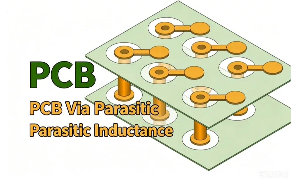
Effect of via inductance on bypass capacitors
The purpose of a bypass capacitor is to short the two power planes together at high frequencies. Suppose an IC is connected between the power and ground planes at point A, and there is an ideal surface-mount bypass capacitor at point B. We expect the high-frequency impedance between the chip pad’s VCC and ground plane to be zero. But in reality it is not. Each via that connects the capacitor to VCC and ground planes adds a small but measurable inductance. The inductance is about:
h = via length (inches)
d = via diameter (inches)
Since the formula has a logarithm, changing the via diameter does not affect inductance much. But changing the via length can cause a big change.
Inductive reactance of a via for a signal with 1 ns rise time. First, calculate the inductance:
- h = 0.063 (via length, inches)
- d = 0.016 (via diameter, inches)
- T10-90% = 1.00 (rise time, ns)
When high-frequency current shunts from the chip, the 3.8 ohm value is not low enough. Also remember, one end of the bypass capacitor is usually connected to the ground plane through a via, and the other end also through a via to the 5V plane. So the effect of via inductance is doubled. Mounting the bypass capacitor on the side of the board closest to the power and ground planes helps reduce this effect. Finally, any lead between the capacitor and the via adds inductance. These traces should always be as wide as possible.
Multiple capacitors in parallel and effective radius
By using many bypass capacitors between power and ground, you can get a very low impedance. For digital products, as a rough standard, assume the power and ground planes are perfect conductors with zero inductance. We only consider the bypass capacitors and their related trace and via inductances. Within a certain range, all bypass capacitors will be connected in parallel, lowering the impedance between power and ground. The effective radius of this effect equals l/12, where l is the electrical length of the rise edge. Within a diameter of l/6, all capacitors work together as one lumped circuit.
In FR-4 material, the propagation length for a 1 ns rise time is about l = 6 in. In this example, if the capacitor grid spacing is larger than l/12 = 0.5 in, there is no benefit.
For power supply bypass capacitors, the shorter the rise time, the harder it is to bypass. When the rise time gets shorter, the effective radius becomes smaller. The number of capacitors within the effective radius decreases with the square of the rise time.
This is a combined problem. As the rise time decreases, the digital corner frequency goes up. This increases the inductance of each via. The final result is: for a certain bypass capacitor configuration working at some frequency, when we cut the rise time in half, its effectiveness drops by a factor of 8. According to scaling rules, experience from one operating frequency range can be easily transferred to a new frequency range.

