


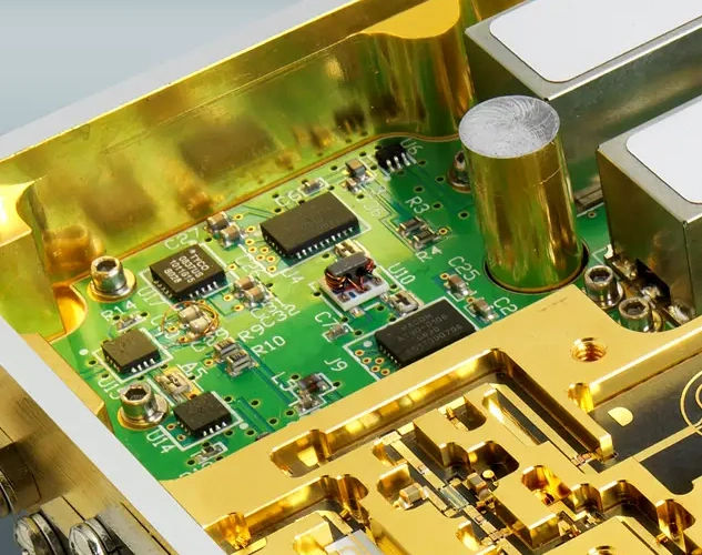
RF PCB je vrsta štampane pločice (PCB) namijenjena za prijenos i obradu radiofrekvencijskih signala. Ovi signali su visoke frekvencije. Obično imaju frekvenciju jednaku ili veću od 300 kHz i do 300 GHz.
Radiofrekvencija, ili RF, je naziv za grupu elektromagnetnih talasa. Ljudi koriste ovaj naziv kada talasi mogu služiti za radio komunikaciju. Opseg frekvencija za RF nije uvijek isti u različitim knjigama. Neke knjige navode da RF obuhvata opseg od 30 MHz do 3 GHz. Neki kažu da je to od 300 MHz do 40 GHz. Ovi rasponi se mogu preklapati s rasponom nazvanim mikrotalasni. Neke druge knjige koriste drugačiji način podjele spektra. Kažu da su u jednoj grupi valovi s valnom dužinom od 1 megametra do 1 metra. To daje frekvencije od 30 Hz do 300 MHz. Granica između RF-a i mikrotalasnih nije vrlo jasna. Granica se može mijenjati kako dijelovi i metode dizajna postaju bolji.
RF PCB i njegove glavne karakteristike
Kada dizajniramo štampanu pločicu (PCB) za RF upotrebu, moramo razmisliti o tome kako se transmisijske linije ponašaju. Za žicu ili trag na PCB-u, možemo ga modelirati na dva načina. Jedan je model zbijenih elemenata. Drugi je model distribuiranih parametara. Opće pravilo je sljedeće. Ako je geometrijska dužina l podijeljena s valnom dužinom λ jednaka ili veća od 0,05, onda koristimo distribuirani model. U ovoj bilješci, RF veza znači sklop gdje prenosna linija zahtijeva distribuirani model. U praksi, dužina staze na PCB-u rijetko je duža od 50 cm. Stoga možemo početi od analognih signala na 30 MHz. Signali iznad 3 GHz često se nazivaju mikrotalasnim. Zbog proizvodnih ograničenja, gdje razmak elemenata može biti 0,5 mm, ljudi ponekad postavljaju gornju frekvenciju na 30 GHz. Ali to nije uvijek korisno.
Na osnovu ovih tačaka možemo reći da je RF PCB štampana pločica za analogne signale čija je frekvencija otprilike od 30 MHz do 6 GHz. Izbor između lumped ili distributed modela treba da se zasniva na gore navedenoj formuli i radnoj frekvenciji.
Budući da je dielektrična konstanta podloge obično visoka, valovi se kreću sporije u ploči nego u zraku. To skraćuje valnu duljinu na ploči. Za mikrostrip i druge vodove podloga mora imati niske dielektrične gubitke. Dielektrična konstanta ne bi smjela znatno varirati u potrebnom frekvencijskom i temperaturnom rasponu. Podloga bi trebala imati dobru toplinsku provodnost i glatku površinu. Mora dobro prianjati uz provodnik.
Za metal na tragu potrebna nam je visoka provodnost. Metal bi trebao imati mali temperaturni koeficijent otpora. Trebao bi se dobro zalijepiti za podlogu. Trebao bi se lako lemiti.
Principi za odabir materijala RF ploče
Uloga podloge u mikrotalasnim tiskanim pločicama
Tiskana pločica mikrotalasne frekvencije nije samo nosač komponenti. Ona je također medij za mikrotalasna elektromagnetska polja. Stoga je za RF kola najbolji izbor visokofrekventni ili mikrotalasni podloga.
Kontrola impedanse traga
Na RF PCB-u tiskani vodovi moraju slijediti uobičajena pravila, poput kapacitivnosti struje. Osim toga, moramo kontrolirati karakterističnu impedanciju vodova. Vodovi moraju biti usklađeni po impedanciji. Dakle, proces izrade PCB-a mora kontrolirati impedanciju vodova. Karakteristična impedancija vodova ovisi o materijalu PCB-a i njegovim fizičkim parametrima. Stoga dizajneri PCB-a moraju poznavati performanse materijala.
Zahtjevi za materijale za RF ploče
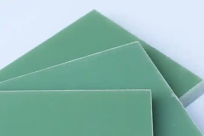
RF ploče obično zahtijevaju visoke frekvencije i visoke performanse. Ljudi biraju podlogu s preciznom dielektričnom konstantom. Podloga treba biti stabilna i imati niske gubitke. Također, materijal mora biti kompatibilan s proizvodnjom. Na primjer, mora izdržati visokotemperaturno taljenje lemom. Naša kompanija često koristi FR4, TACONIC i materijale iz ROGERS-a za RF bazni materijal.
FR-4 karakteristike
FR4 (epoksidno stakleno tkivo sa bakrenom oblogom i plamenom otpornim svojstvima) ima dielektričnu konstantu Er ispitanu na 1 GHz kao Er = 4,3 ± 0,2. Stakleni prijelazni temperatur Tg je 135 °C. Za uobičajene ploče koristimo dvije vrste ploča. Jedna je standardni materijal za ploče. To je jeftino i ima zreli proces. Druga je UV ploča, često nazvana žuta ploča. Ima UV-BLOKIRANJE za blokiranje ultraljubičastog zračenja. Koristimo je za vanjske slojeve. Njena performansa je malo bolja od standardne ploče.
TACONIC materijal
Takonički je dobro poznat brend. Ima mnogo specifikacija. Njegova cijena je viša od fr4.
ROGERS materijal
ROGERS materijal ima visoku tačnost dielektrične konstante. Stabilan je na temperaturi i ima niske gubitke. Koristimo ga za kola visoke snage. Proizvodnja i obrada PCB-a su slični onima za FR4, pa je trošak izrade nizak. Međutim, adhezija bakarne folije je slaba.
Tabela supstrata
| Vrsta materijala | Tipični materijal | Dk (10 GHz) | Df (10 GHz) | Karakteristike i upotreba |
|---|---|---|---|---|
| Fluoropolimerni podloga | PTFE (politetraflouroetilen) | 2.1–2.3 | 0.0005–0.001 | Vrlo niski gubici. Pogodno za mmVal. Koristi se za 5G bazne stanice i radar. |
| Podloga ispunjena keramikom | Rogers serija RO4000 | 3.38–4.5 | 0.0027–0.004 | Srednja cijena. Pogodno za mikrotalasnu pećnicu. Koristi se za WiFi i Bluetooth module. |
| Podloga od staklenih vlakana | Visokofrekventni FR4 (kao Isola FR408) | 3.9–4.2 | 0.008–0.01 | Niska cijena. Dobro za srednji i niski RF. Koristi se za voki-tokije i slično. |
RF problemi u dizajnu štampanih pločica i rješenja
Općenito, za kola s frekvencijom ispod mikrotalasne (što uključuje niskofrekventna i digitalna kola niske brzine), pažljiv raspored je prvi ključ uspjeha. Ako poznajete pravila, možete napraviti dobar dizajn. Za mikrostrip i visokobrzinska digitalna kola na nivou PCB-a mogu biti potrebne dvije ili tri verzije PCB-a kako bi se osigurala kvaliteta kola. Za RF kola s frekvencijom iznad mikrotalasne, trebat će vam više verzija za poboljšanje performansi. Dakle, suočit ćete se s mnogim izazovima tokom dizajna RF kola.
U nastavku navodimo uobičajene probleme i rješenja.
Uobičajeni problemi u dizajnu RF sklopova
Interferencija između digitalnih i analognih modula
Kada analogni RF i digitalni dijelovi rade odvojeno, svaki može raditi dobro. Ali kada se pomiješaju na istoj ploči i dijele napajanje, cijeli sistem može postati nestabilan. Digitalni signali osciliraju između mase i Vcc za više od 3 V. Period može biti kratak, u nanosekundnom rasponu. Zbog velike amplitude i brzog prebacivanja, digitalni signali sadrže visokofrekventne komponente koje ne ovise o taktu prebacivanja. U analognom dijelu, od podešene radio petlje do prijemnika, napon može biti manji od 1 μV. Razlika između malog RF signala i digitalne buke može biti veća od 120 dB. Ako se digitalni signali ne drže podalje od RF-a, slab RF signal može biti oštećen. Radio može prestati raditi ili raditi loše.Smetnje od buke napajanja
RF sklopovi su osjetljivi na šum. Osjetljivi su na skokove napona i druge visokofrekventne harmonike. Mikro kontroler će iznenada povlačiti veliku struju u svakom unutrašnjem taktu. Većina modernih mikrokontrolera koristi CMOS. Ako mikrokontroler radi s internim taktom od 1 MHz, vući će struju tom brzinom. Ako nemamo dobro odvođenje napajanja, doći će do šuma napona na linijama napajanja. Ako naponski skokovi dospiju do RF pinova za napajanje, RF blok može otkazati.Loš dizajn tla
Ako masa nije dobro dizajnirana za RF, mogu se dogoditi čudni rezultati. U digitalnom dizajnu većina kola i dalje radi čak i ako masa nije savršena. Ali u RF-u čak i kratki vodovi za masu ponašaju se kao indukтори. Na primjer, 1 nH indukancije odgovara otprilike 1 mm duljine. Iz toga možemo pretpostaviti da traga na PCB-u dužine 10 mm ima reaktansu od oko 27 ohma. Ako nemamo dobru masu, mnoge trage za masu bit će duge i kolosijek neće zadržati svoje projektirane karakteristike.Zračenje antene koje ometa druge analogne sklopove
U rasporedu štampane pločice postoje i drugi analogni dijelovi. Mnoge pločice imaju ADC ili DAC. Snažan RF signal iz predajnika može dospjeti do ulaza ADC-a. Svaki vod može djelovati kao antena. Ako ulaz ADC-a nije dobro zaštićen, RF može ući u njegovu ESD diodu i uzrokovati pomak ili greške u ADC-u.
Principi i rješenja za dizajn RF kola
1. Definicija RF rasporeda
Kada dizajnirate RF raspored, slijedite ova pravila.
Držite pojačala velike snage (HPAs) i pojačala niskog šuma (LNAs) što je moguće dalje jedno od drugog. Postavite komponente za prijenos velike snage daleko od komponenti za prijem male snage.
Na visokofrekventnim područjima na PCB-u imajte najmanje jednu punu uzemljivu ravan ispod i izbjegavajte vijase u njoj. Što je veća bakrena površina, to je bolje.
Rasipanje struje i odvajanje napajanja su jednako važni.
Postavite RF izlaze podalje od RF ulaza.
Postavite osjetljive analogne signale daleko od brzorazrednih digitalnih i RF signala.
2. Pravila za projektovanje fizičke i električne particije
Particija znači razdvajanje ploče po funkciji. Možete napraviti fizičku i električnu particiju. Fizička particija se bavi rasporedom dijelova, smjerom i zaštitnim pločama. Električna particija se bavi raspodjelom napajanja, RF rutiranjem, osjetljivim dijelovima, signalima i zonama uzemljenja.
a. Principi fizičke podjele
Raspoređivanje komponenti je ključno za dobar RF dizajn. Dobra metoda je prvo postaviti komponente duž RF puta. Zatim postavite njihov smjer. Postavite ulaze podalje od izlaza. Držite komponente visoke i niske snage odvojeno. To pomaže skratiti RF puteve.
b. Princip dizajna slojeva PCB-a
Dobar stackup postavlja glavnu uzemljivu ravan na sloj ispod sloja tragova. Postavite RF tragove na ravan. Napravite male vias na RF putanjama. To smanjuje induktanciju putanje i broj hladnih lemnih spojeva na glavnom uzemljenju. Također će manje RF energije curiti u druge slojeve.
c. RF dijelovi i principi RF tragova
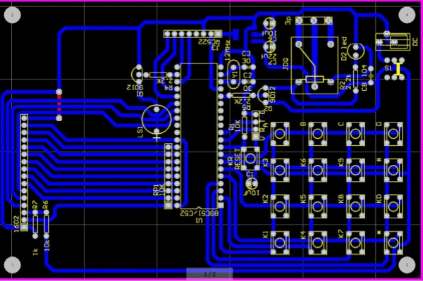
U prostoru za ploču, linearni krugovi poput višestupanjskih pojačala mogu odvojiti RF zone. Ali duplexeri, mikseri i IF pojačala često dovode do toga da se mnogi RF i IF signali pojavljuju blizu jedni drugih. Trebate paziti da smanjite ovo uzajamno djelovanje. Provedite RF i IF tragove pažljivo i ostavite prostor za uzemljenje između njih. Ispravan RF put je ključan za performanse PCB-a. Zato raspored komponenti oduzima većinu vremena pri dizajniranju PCB-a za telefone.
d. Princip električne pregrade
Većina napajanja u telefonskim krugovima je niskog istosmjernog napona, pa vam nisu potrebne posebne široke staze. Ali za napajanje visokosnažnih pojačala morate napraviti široke staze zbog velikog strujnog opterećenja. Time se pad napona održava niskim. Koristite mnogo vias da biste preusmjerili struju s jedne ravni na drugu i izbjegli gubitak struje.
Odspajanje napajanja za komponente visoke snage je važno. Ako ne uspijete odspojiti napajanje na pin visokosnažnog pojačala, mogu se pojaviti mnogi problemi. Šum visoke snage može se širiti po ploči. Masa za visokosnažna pojačala je vrlo važna. Projektanti često trebaju metalnu zaštitnu kutiju.
e. Princip izolacije RF ulaza/izlaza
Vrlo je važno držati RF izlaz podalje od RF ulaza. Ovo se odnosi na pojačala, bufere i filtre. U najgorem slučaju, ako se izlaz pojačala ili bufera vrati na njegov ulaz s pravom fazom i amplitudom, komponenta može ući u samoresonanciju. U najboljem slučaju, sklop će biti stabilan pri svim temperaturama i naponima. U lošem slučaju, on će dodati šum i intermodulaciju RF signalu.
Sažetak
Ukratko, RF kola rade s linijama distribuiranih parametara. Pokazuju kožni efekt i uzajamno djelovanje. To ih čini različitim od niskofrekventnih i istosmjernih kola. Dakle, pri dizajniranju RF PCB-a morate se usredotočiti na gore navedene tačke. Ako to učinite, dizajn će biti učinkovit i precizan.
Držite tragove kratkim kad god je to moguće. Kratki tragovi smanjuju gubitke i neželjenu reaktanciju.
Koristite odgovarajući supstrat za potrebnu frekvenciju. FR4 je prihvatljiv u mnogim slučajevima. Koristite Rogers ili PTFE za niske gubitke na visokim frekvencijama.
Kontrolirajte impedanciju tragova. Koristite odgovarajuću širinu, razmak i slojevnu strukturu. Mjerite ili izračunajte pomoću alata.
Držite digitalne i RF komponente odvojeno. Svakom dijelu osigurajte vlastiti povratni vod za masu. Koristite dekupiranje na pinovima za napajanje blizu komponente.
Koristite uzemljene ravnine i male vijase za povrat RF-a. To smanjuje induktansu.
Postavite filtre i zaštitu u blizini osjetljivih dijelova. To smanjuje neželjeno primanje smetnji.
Testirajte s prototipovima. RF obično zahtijeva više krugova rasporeda i podešavanja. Male promjene mogu imati velike efekte na visokim frekvencijama.
Za antene osigurajte dovoljno slobodnog prostora i držite metalne i druge tragove podalje. Prilagođavanje i podešavanje antene često zahtijevaju prostor na ploči i testiranje.
Kada pravite staze visoke snage, napravite ih širokima i koristite mnogo via za provođenje struje između slojeva.
Osnovne formule i pravila za provjeru
Koristite l/λ ≥ 0,05 da biste provjerili treba li tragu distribuirani model. l je geometrijska dužina. λ je radna valna duljina u mediju.
Za brzo mjerenje indukancije, 1 nH je otprilike 1 mm staze. Koristite ovo da provjerite da li duge uzemljene staze dodaju indukanciju.
Za kontrolu impedanse, poznajte slojevitost, širinu trake, dielektričku konstantu i udaljenost od ravnine. Koristite rešavač polja ili kalkulator impedanse da biste dobili tačne vrijednosti.