
RF & Microwave PCB Manufacturing
The RF circuit. Its ground. Its connections.
FLJ manufactures RF and microwave PCBs for communication, sensing and instrumentation. From transmission-line patterns to plated ground connections and connector interfaces, we build the physical board that carries your RF circuit.
Prototype & production · Bare boards & PCB assembly
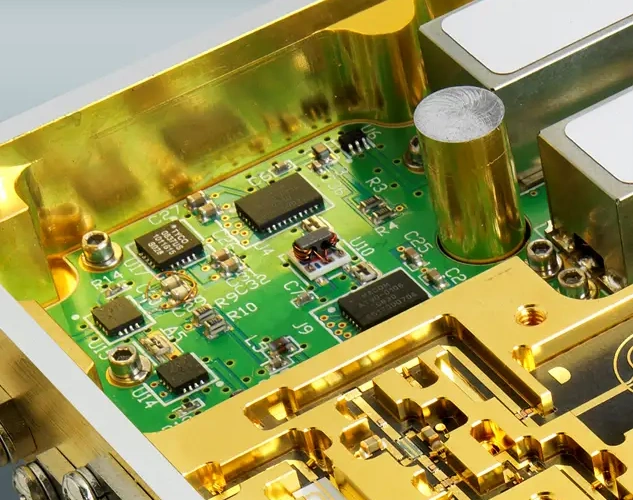
RF and Microwave Boards We Manufacture
RF circuitry may occupy a dedicated board or share a multilayer PCB with digital control and power. FLJ supplies both the bare circuit and its populated assembly, with the material, interconnections and mechanical features suited to the product.
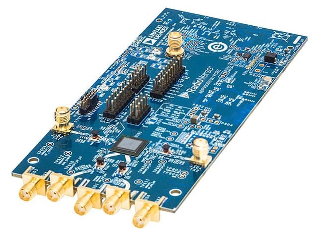
Fabricating RF Circuit Structures and Connections
An RF transmission line includes the signal conductor, its reference conductors and the dielectric between them. Fabrication creates that structure, including the copper beside the trace, the connections between layers and the interface at the board edge.
Form the line and the copper around it
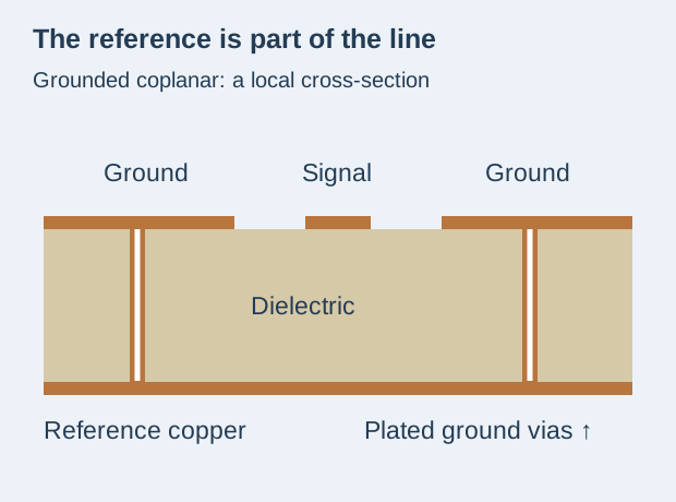
Microstrip uses a surface conductor with a reference plane below it. Stripline places the conductor between reference planes. Grounded coplanar waveguide adds ground copper beside the surface trace, with plated vias connecting that copper to the reference plane.
Imaging and etching form both the RF line and the copper beside it. Where adjacent conductors form part of the circuit, the gap between them is an electrical feature as well as a manufacturing clearance. Etch compensation accounts for copper thickness and sideways removal at the conductor edges, connecting the production artwork to the finished line and gap. The pressed dielectric spacing completes the physical geometry.
Make the reference connection part of the build
Ground vias connect surface copper to the reference structure inside the PCB. Drilling and plating turn the indicated hole pattern into copper connections through the selected layers. Around an RF line or transition, these connections give return current a path between the conductors that form the ground structure.
A signal via carries the circuit through its pad and plated barrel to another layer. The associated reference connection has to transfer with it. Through, blind or buried connections are selected within the stackup, with their copper lands and plane openings formed as part of the complete transition.
The via is also a feature in every layer it passes through. Pads and clearance openings have to fit within the internal copper pattern. Dense through-hole clearances can interrupt a plane, so via construction and layer registration are considered together with the circuit geometry.
Fabricate the transition at the board edge
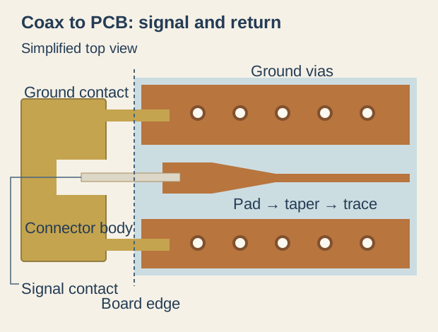
A coaxial connector joins more than a center pin to a trace. Its signal contact meets a pad and transition, while its ground contacts connect the outer conductor to PCB ground.
FLJ fabricates the launch pads, taper, ground copper and plated connections in the selected construction. Routing defines the board edge and contact position. The connector’s mounting geometry and the board thickness complete the mechanical fit.
A wider signal pad changes the local capacitance, while a long or poorly connected return path adds parasitic inductance. The pad, taper, reference clearance and ground contacts therefore act together at the interface. Their exact shapes follow the connector and stackup; the connector’s nominal impedance alone does not define the assembled launch.
Materials, Stackups and Surface Options
PTFE-based, hydrocarbon ceramic and selected low-loss laminates provide different electrical and processing options. The material grade, copper and layer construction work together in the finished RF circuit.
Dielectric values are used with their frequency and test-method context. A familiar material name or a low Dk value alone does not describe the loss or impedance of the complete board.
High-frequency materials & fabrication →| Element | What it defines in the circuit |
|---|---|
| Laminate & bonding system | Electrical material properties and the construction that joins the layers |
| Reference & spacing | The copper reference beside each RF path and its finished dielectric separation |
| Copper foil & finished circuitry | Conductor surface, thickness, line shape and gaps |
| Mask & surface finish | Covered areas, exposed RF conductors, solder pads and contact surfaces |
| Board edge & thickness | Connector seating, contact height and fit with the surrounding assembly |
Finish choices are made with the RF structure and its soldering or contact function in view.
RF PCB Assembly and Verification
Fabrication and assembly bring the board geometry, components and connectors together. FLJ combines PCB manufacturing with component sourcing and assembly for a coordinated prototype or production build.
Carry the interface through assembly
Connector placement follows the board edge and its mounting geometry. Solder joins the signal contact to its pad and the ground contacts to their copper areas. Wetting, contact seating and the shape of the finished joints all contribute to the physical RF transition.
At a launch, additional solder changes the metal shape as well as the mechanical joint. Controlled application and inspection preserve the intended connection. The populated board is then ready for the selected inspection and test sequence.
Board structure & connections
Optical inspection checks conductor features; electrical testing checks opens and shorts. Local sections can show internal copper connections and plated-hole structure.
Controlled-impedance features
Representative test coupons support verification of defined transmission-line geometry. This complements the physical and electrical network checks.
RF characterization
RF characterization evaluates reflection and transmission over the selected ports and frequency band. Calibration establishes the reference planes. Connector launches and fixtures remain part of the measured response unless their effects are removed through an appropriate de-embedding method.
RF and Microwave Applications
Communication links and RF instruments depend on the relationship between the circuit, its reference structure and its interfaces.
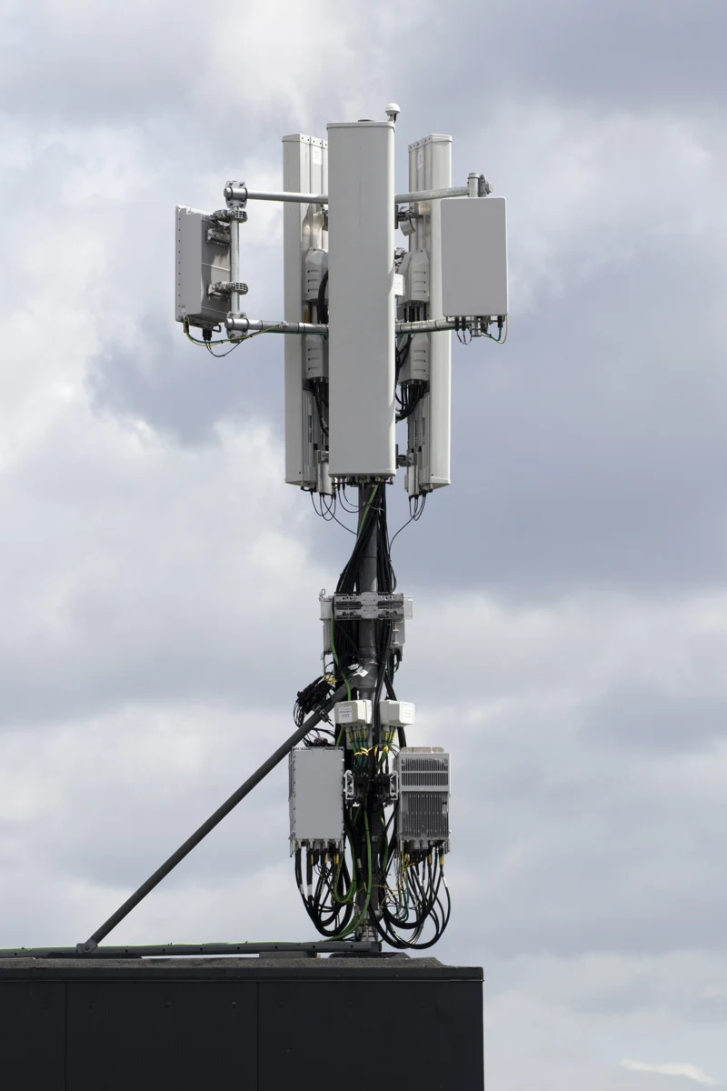
Communication & wireless infrastructure
RF front ends, antenna feeds and radio links combine signal processing with connections to the wider system. Dedicated or mixed-function boards support the RF section within that hardware.
RF instrumentation & sensing
RF signal generation, measurement and sensing systems use defined signal paths, transitions and reference structures. Board fabrication and connector assembly carry those features into the finished electronics.
Build your next RF board with FLJ.
Choose bare-board fabrication or a populated RF assembly. The selected laminate, stackup and connector interface remain defined parts of the build as a prototype moves into production, with changes carried through fabrication and assembly together.
Related RF PCB designs
Explore the board images, product information and design details for related projects.


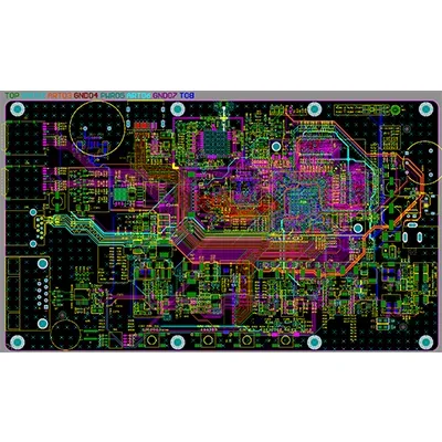
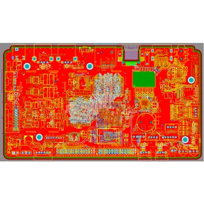
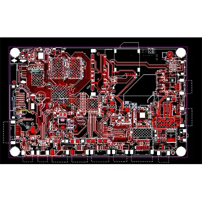
Medical X-Ray Equipment RF PCB Design
An RF PCB design profile for medical X-ray equipment.
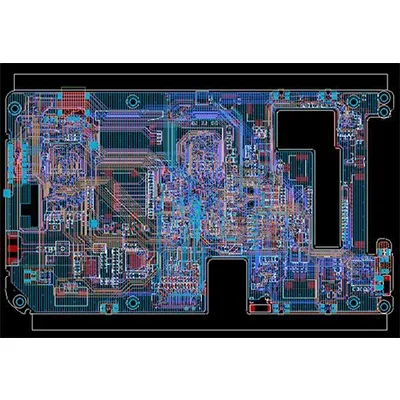
Automotive Multilayer RF PCB Design
A multilayer RF PCB design profile for automotive electronics.