


Pregled
Elektronički proizvodi postavljaju veće zahtjeve pred tiskane pločice. Broj komponenti na ploči brzo raste. Veličine komponenti postaju sve manje. Polu-rupe na tiskanim pločicama sve se više koriste jer se lako lemaju, zauzimaju malo prostora na modulu i podržavaju mnoge funkcije.

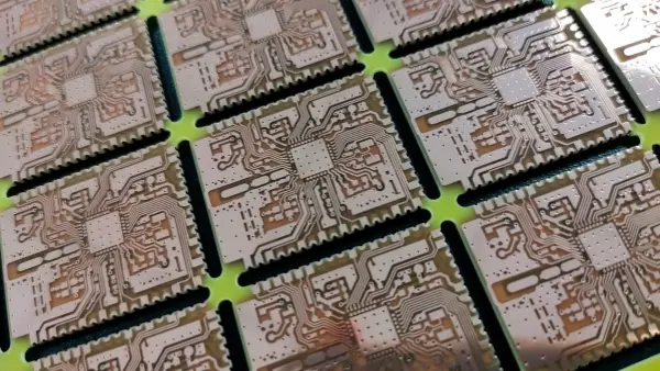
Šta je polu-rupa na štampanoj pločici?
Metalni polu-otvor (ili polu-prorez) se pravi tako što se prvo bušenje i metaliziranje rupe, zatim ponovno bušenje ili freziranje kako bi se rupa prepolovila. Jednostavno rečeno, to je metalizirana rupa na rubu ploče prepolovljena. Proces rubne polumetalizirane rupe je zreo. U industriji tiskanih pločica ovo se također naziva “rupa veličine poštanske marke”. Rub rupe možete direktno zalemiti na glavnu ploču. Time se štedi na konektorima i prostoru. Često se susreće u signalnim krugovima. Većina PCB-ova za module koristi polu-rupe.
Karakteristike metaliziranih PCB-ova s polupropusnim rupama
Jedinica je mala.
Rub jedinice ima red metaliziranih polu-rupa. Ova jedinica je podloga na matičnoj ploči. Metalizirane polu-rupe se lemom spajaju na matičnu ploču i na izvođe komponente.

Prednosti polu-rupe procesa
Povećajte čvrstoću jastučića. Dizajn polu-rupe mehanički ojačava rubni kondenzator. Kod modularnih tiskanih pločica poboljšava pouzdanost lemljenja. Pogodan je za primjenu u okruženjima visoke gustoće i visokih vibracija.
Optimizirajte raspored prostora. Polupropusni otvori omogućavaju fleksibilnije postavljanje dijelova i manje zauzimaju prostor. Na primjer, kod Wi-Fi modula možete lemiti rubni polupropusni otvor direktno na glavnu ploču i smanjiti debljinu proizvoda za otprilike 60%. Ovo odgovara tankim uređajima.
Pojednostavite proizvodnju. Proces zahtijeva dodatne korake na početku (na primjer, bakarnu pozlatku i precizno razdvajanje), ali je sveukupno efikasniji od upotrebe tradicionalnih konektora. Također izbjegava kupovinu konektora.
Poboljšajte izgled. Rupe na rubu pločice čine da izgleda urednije. To zadovoljava suvremene zahtjeve za izgledom proizvoda.
Poboljšajte performanse signala. U visokofrekventnim slučajevima (na primjer 5G) polurupe mogu smanjiti parazitsku kapacitivnost i smanjiti gubitak signala. To povećava efikasnost prijenosa.
Teškoće u obradi
Nakon oblikovanja, metalizirane PCB ploče s polu-otvorima često pokazuju probleme na zidovima rupa od bakra. To uključuje odvajanje bakra, tamni bakar, preostale žljebove i pomicanje. Ovi problemi predstavljaju uobičajeni izazov za proizvođače PCB-a u fazi oblikovanja.
Puna linija polurupa nalik poštanskoj marki posebno je teška. Veličina rupa je oko 0,6 mm. Razmak između rupa i njihovih zidova je oko 0,45 mm. Razmak uzoraka na vanjskom sloju je oko 2 mm. Mali razmaci olakšavaju kratka spojena zbog Kuperove kože.
Uobičajene metode oblikovanja metaliziranih polu-rupa na PCB-ovima uključuju CNC glodanje (glodalica), mehaničko probijanje i V-rezanje. Kada ove metode uklanjaju nepotrebne dijelove obloženih rupa, često ostavljaju bakrene niti i žljebove na rezanim rubovima PTH (obloženih prolaznih rupa). U ozbiljnim slučajevima bakar na zidovima rupa može se odvojiti ili ljuštiti. Također, tokom oblikovanja, širenje PCB-a, preciznost položaja bušilice i preciznost oblikovanja mogu uzrokovati da polurupe s lijeve i desne strane iste jedinice znatno razlikuju u veličini. To otežava klijentima lemljenje i montažu.
Napomene za proces polu-rupa na PCB-u
Sve pozicije polu-rupa na metaliziranim PCB-ovima moraju biti izbušene nakon slikanja/galvanizacije (ili nakon uzorkovane galvanizacije), i prije graviranja, tako da na svakom kraju polu-rupe presjeke bodova bude izbušena rupa.
Odjel za inženjering treba postaviti tok MI (uputstva za proizvodnju) za proces polu-rupe.
Za metalne polu-rupe koje se formiraju prvo bušenjem (ili fréziranjem), zatim platingom po uzorku, pa drugim bušenjem prije etsiranja, razmislite hoće li vanjsko oblikovanje (routing) izložiti bakar. Ako je potrebno, pomaknite izbušenu polu-rupu prema unutrašnjosti jedinice.
Za rupu na desnoj strani (izbušena polurupa):
a. Prvo izbušite, zatim okrenite ploču (ili je ogledajte) i izbušite rupu na lijevoj strani.
b. Ovo smanjuje vučenje burgija na bakar u rupi i sprječava gubitak bakra unutar polurupe.Veličina burgija za polupolje ovisi o udaljenosti od konturne linije.
Nacrtajte film za masku za lemljenje. Za izrezane otvore dodajte zaustavne tačke i povećajte prozore za 4 mil.
Tok procesa
Polurupa je metalizirana rupa izrezana na pola. Izgleda jednostavno jer biste mogli pomisliti da trebate samo izfrézirati obris na običnoj ploči. Zapravo, to nije jednostavno.
Frezirajte polu-rubne rupe koristeći dvostruku V-oblikovanu putanju rezanja.
Za drugo bušenje dodajte vodične rupe na rubu prekinute rupe. Rano uklonite bakreni sloj kako biste smanjili žljebove. Pređite s ravne svrdle na rezač utora i optimizirajte brzinu vretena i napajanje.
Nanesite bakrenu prevlaku na ploču tako da zidovi okrugle rupe na rubu ploče dobiju sloj bakra.
Napravite vanjski sloj pločice tako što ćete laminirati, izlagati i razvijati. Zatim nanesite drugo presvlačenje bakrom i kalajem kako bi sloj bakra na zidovima okrugle rupe na rubu postao deblji i bio prekriven slojem kalaja koji otporan na etsiranje.
Oblikujte polu-otvor tako što ćete okrugli otvor na ivici ploče prepoloviti.
Uklonite sloj otporničke folije koji je pritisnut tokom laminacije.
Gravirajte ploču da uklonite izloženi vanjski bakar koji je ostao nakon skidanja maske.
Ogoli lim na ploči tako da bakar na zidu polu-rupe bude izložen.
Nakon formiranja, upotrijebite crvenu traku da držite pločice jedinica zajedno. Prođite ih kroz alkalno graviranje kako biste uklonili žljebove.
Nakon što ploča dobije drugu bakarnu i kalajnu prevlaku, prerežite okrugli rubni otvor napola kako biste dobili polu-otvor. Budući da je bakrena stijenka otvora prekrivena kalajem i potpuno povezana s bakrom vanjskog sloja, veza je čvrsta. Rezanje potom sprječava podizanje ili ljuštenje bakra.
Nakon što se formiranje polu-rupa završi, uklonite zaštitni sloj i zatim izgradiite. To sprječava oksidaciju bakra na površini i izbjegava ostatke bakra ili čak kratka spojevanja. Povećava iskoristivost metaliziranih polu-rupa na PCB-ovima.