
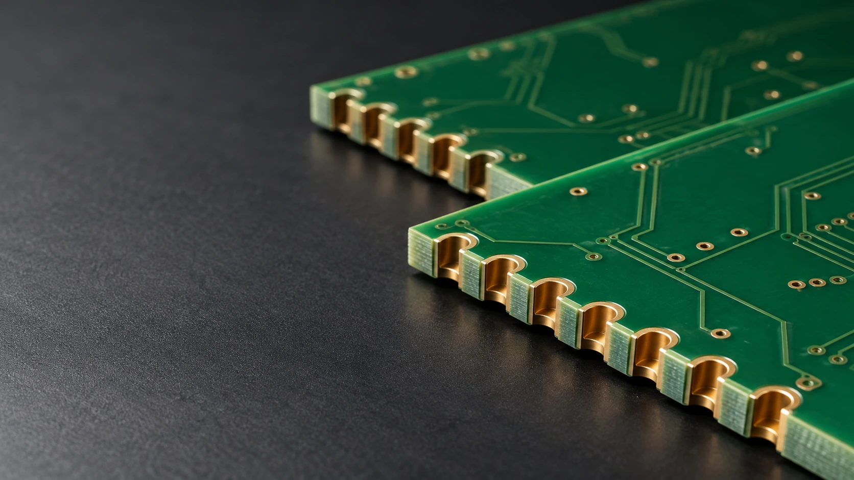
Plated half-hole PCB fabrication
Castellated PCB
Manufacturing
A solderable edge.
A direct connection to your host board.
FLJ manufactures castellated PCBs for modules that solder directly onto a larger board. From prototype builds to production, the plated holes, supporting lands and finished profile are fabricated as one connected edge feature.
Built around the module edge
Solderable Edge Connections for PCB Modules
The Half-Hole, Copper Land and Host Pad
A castellation exposes part of a plated hole at the finished PCB edge. Its remaining copper wall connects to the module’s designated lands and creates a solderable interface to the host board. The open recess allows solder to reach the edge contact when the module is mounted.
FLJ supplies these features as part of the board fabrication, combining the hole pattern, copper lands, profile and finish. Rectangular modules, shaped boards and repeated contact rows can be developed around the space available in the finished product.
Wireless and control modules use this construction to bring a functional circuit onto a larger PCB without a separate board-to-board connector. The module still needs a matching host footprint: its pads must receive the finished contacts at the intended placement position.

The wall copper provides the edge contact. Copper lands anchor it to the module. The host pad and solder joint complete the connection during assembly.
A plated half-hole remains in the product. Mouse-bite perforations serve a different purpose: they help separate a board from its temporary panel support.
From an intact hole to a finished contact
Manufacturing Plated Half-Holes
The operation has to open the board edge while keeping the copper that makes the contact useful. Hole metallization, profile machining and edge finishing work together to produce that result.
Forming and Plating the Complete Hole
Drilling establishes the hole before its wall is opened at the board perimeter. Hole-wall preparation and metallization form a conductive barrel, and copper lands connect that barrel to the intended circuit layers.
The plated hole and the final outline share the same manufacturing coordinates. Defining them together establishes where the future edge will cross the hole and which part of the contact must remain on the delivered board.
Supporting the Copper During Profiling
Profile machining removes the outer portion of the plated hole. As the cutter opens the wall, the remaining sleeve needs support from the laminate and copper lands. Tool approach, cutting path and panel support affect whether the copper remains attached or lifts at the edge.
FLJ prepares the profile operation around the contact row and its supporting copper. Where inner-layer lands contribute mechanical support, their electrical connections and clearances follow the circuit design. Adding support does not mean joining every layer to the contact.
Cleaning and Inspecting the Finished Edge
Machining residue and unwanted copper fragments are removed from the opened edge. The finished contact is examined for wall continuity, lifted copper, land damage and burrs that could interfere with soldering or bridge adjacent contacts.
Dimensional checks relate the finished outline to the hole and retained land. PCB electrical testing checks the intended connections and isolation; physical edge inspection addresses the condition of the contact that will later receive solder.
Hole · land · profile · construction
Hole, Land and Outline Specifications
Diameter, Pitch and Retained Copper
Hole diameter determines the initial opening. Contact pitch sets the space between neighboring holes, while the surrounding land provides copper support and a solderable surface. The final outline decides how much of each hole and land remains.
These dimensions belong together. Enlarging a land can improve its supporting area while reducing the copper gap to the next contact. Moving the outline relative to the hole changes recess depth, even when the visible opening width changes very little.
Board Thickness, Finish and Layer Connections
Castellated boards can be supplied in FR-4 constructions with the selected Tg grade and copper arrangement. ENIG, OSP and other supported finishes are selected with the exposed contact, storage and assembly process in mind. The chosen finish covers the specified solderable surfaces; the hole-wall copper remains a separate part of the construction.
Scroll to see each specification and its relationship →
| Specification | What it describes | How it affects the supplied board |
|---|---|---|
| Finished hole & contact pitch | Diameter, row spacing and neighboring contacts | Coordinates the recess size, supporting land and space between contacts. |
| Outline & retained land | Final profile relative to the hole and copper | Controls the exposed contact and the copper retained on the module. |
| Material, Tg & thickness | Laminate and finished board construction | Sets the physical module edge and the structure being profiled. |
| Copper connections | Connected lands and isolated layers | Preserves the intended electrical network and local copper support. |
| Surface finish | ENIG, OSP or another supported finish | Matches the exposed solderable contact to the assembly requirement. |
| Delivery form | Panelized boards or separated modules | Coordinates contact protection, handling and downstream placement. |
See our PCB manufacturing capabilities for the wider fabrication range. The half-hole dimensions are evaluated as a complete construction, rather than by combining unrelated process limits.
Interactive design preview
Half-Hole Geometry & Land Spacing
Explore how the board edge cuts a circular hole, then check the space between neighboring contacts. All dimensions are in millimeters.
- Opening at selected edge
- Recess at selected edge
- Full pad diameter (nominal) D + 2A, before profile clipping
- Full pad gap (nominal)
The example dimensions are not FLJ capability limits. Opening and recess bounds describe the dimensions produced as the edge varies over e ±t. Hole diameter, pitch and land width remain fixed. The spacing results are nominal: diameter, pitch and land-registration tolerances are not included. Copper thickness and the final clipped-land shape are outside this model.
Calculation method
For radius r = D/2 and edge coordinate e, opening width is 2√(r² − e²) and inward recess depth is r − e. The preview evaluates the interval e − t to e + t. Opening width reaches D when that interval includes the hole center; its minimum occurs at the endpoint farther from the center.
Inputs stay in this browser. Download the brief and attach it to your enquiry if useful; the tool does not submit a design or calculate a manufacturing price.
Fabrication through to integration
Panel Delivery and Module Assembly
Protecting the Contact Edge in a Panel
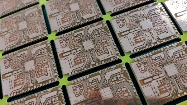
A panel holds the modules stable during manufacture and handling. Its support bridges and separation areas must leave the intended solderable edges intact. A row of permanent plated contacts and a row of temporary breakaway holes have different jobs, even when both sit near an outline.
FLJ supplies panelized boards or separated modules to suit the next operation. Panel arrangement, routing access and the separation path are coordinated around the contact locations, including layouts with contacts on more than one edge.
Routing channels leave the plated contact edges exposed, while temporary bridges hold the module at available non-contact locations. The separation path crosses those bridges, rather than the permanent contact row. That placement preserves the solderable edge during removal from the panel.
Where contact rows occupy several sides, the remaining support locations and machining access are planned together. The delivered outline is the module perimeter after the temporary supports have been removed.
From Finished Module to Host Board
The host pads need suitable overlap, placement clearance and solder access around the completed module. FLJ can carry the board into SMT assembly, connecting fabrication and module mounting within the same production project. The fabrication and assembly review can address the relationship between the two board drawings before manufacture.