
CERAMIC CIRCUITS · CUSTOM FABRICATION
Ceramic PCB
Manufacturing
Electrical insulation.
A direct role in thermal design.
FLJ manufactures ceramic circuit boards, optoelectronic submounts and power substrates. Combine alumina, aluminum nitride or silicon nitride with the conductor structure your device needs, supplied as patterned bare boards or populated assemblies.
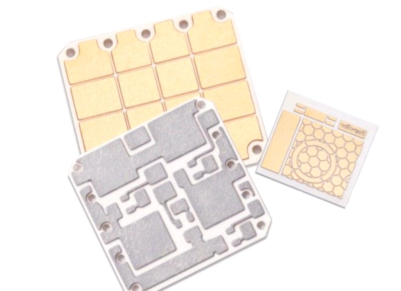
Fine circuits, power substrates and printed hybrids.
Prototype and production supply.
THE CIRCUIT, THE SUBSTRATE, THE DEVICE
Ceramic PCB Products and Circuit Structures
Ceramic provides the electrically insulating base; patterned metal provides the connections. The conductor can be plated, bonded or printed, creating different products for component mounting, power switching and hybrid electronics.
FINE CIRCUITS & OPTOELECTRONICS
Component boards and submounts
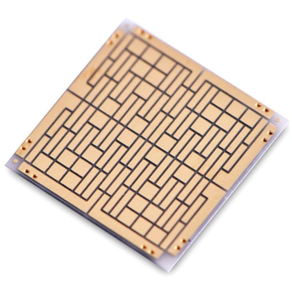
LED emitters, laser diodes and photodetectors need accurately positioned contacts on a compact carrier. Direct plated copper (DPC) forms separate tracks and pads on a fired ceramic surface, carrying electrical connections while the substrate conducts heat toward the mounting surface.
Alumina offers an established ceramic platform for component circuits. Aluminum nitride adds higher substrate thermal conductivity for more concentrated heat loads. The pad layout, circuit metal and selected finish accommodate the device connections; FLJ supplies the patterned carrier or extends the build through component sourcing and PCB assembly.
POWER ELECTRONICS
Copper / ceramic power substrates
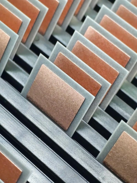
IGBT and SiC power modules use patterned copper for device attachment and current distribution. The ceramic electrically separates this live circuit from the cooling structure while conducting heat through the substrate. In a double-sided construction, rear copper provides a further heat-spreading and attachment surface. These substrates serve motor inverters, power converters and industrial drives where heat leaves through the base of the module.
Direct bonded copper (DBC) and active metal brazed (AMB) constructions join copper sheet to ceramic before the circuit is etched. Alumina, AlN and silicon nitride bring different thermal and mechanical properties to that structure. Copper thickness, conductor spacing and the joining interface are developed together for the power circuit.
PRINTED FUNCTIONAL CIRCUITS
Thick-film and hybrid ceramic circuits
Screen-printed conductor and resistor pastes turn the ceramic into a functional circuit carrier. Successive printing and firing operations create interconnections and resistive elements; laser trimming can adjust a fired resistor to its target value. Mounted semiconductors and other components complete the hybrid.
This construction supports sensor interfaces, resistor networks and heater circuits, bringing functions onto the substrate that a copper pattern alone does not provide. Conductor, resistor and protective materials form a compatible firing system. The photograph illustrates this circuit type rather than a FLJ customer project.
MATERIAL PROPERTIES THAT SHAPE THE CIRCUIT
Alumina, Aluminum Nitride and Silicon Nitride
Thermal conductivity helps compare heat flow through the ceramic. Expansion and mechanical behavior matter too: the ceramic, copper and attached device move differently as temperature changes.
| Ceramic | Thermal conductivity W/m·K at 20°C | Linear expansion ppm/K, 100–800°C | Product selection |
|---|---|---|---|
| 96% alumina Al2O3 | 24 | 7.0–9.0 | Established, economical base for printed hybrids and component carriers when its thermal performance meets the design. |
| Aluminum nitride AlN | 170 | 4.8–6.2 | Higher heat conduction through the substrate for concentrated heat sources, including LED and laser submounts. |
| Silicon nitride Si3N4 | 90 | 3.3 | Mechanical robustness alongside heat conduction for power substrates exposed to repeated thermal loading. |
Values represent particular substrate grades, rather than all grades in each family. Conductivity is measured by Xe-flash on 16 × 16 mm material samples; sample thickness varies by grade. The material data carry a ±10% measurement tolerance. The expansion test interval is a measurement condition, not a board operating-temperature rating.
Heat must pass through the complete structure
For one-dimensional heat flow through a uniform layer, thermal resistance follows R = t / (k × A): thickness increases resistance, while conductivity and cross-sectional area reduce it. Heat spreading in a real circuit makes the geometry more complex. A device on a ceramic board also has die-attach or solder interfaces, patterned metal and a connection to the cooler. Their contact areas and bond quality influence the finished thermal path.
An AlN submount can therefore improve the substrate portion of an LED or laser package without making every other thermal interface disappear. Where a metal base with a polymer dielectric suits the design, metal core PCB constructions offer a different route for lighting and power boards.
Expansion becomes an interface issue
Heating and cooling create strain between materials with different coefficients of thermal expansion. Copper geometry, ceramic toughness and the bonding layer affect how that strain is distributed. Silicon nitride is valued in power substrates for its mechanical robustness as well as its thermal properties.
AlN leads this comparison in thermal conductivity; silicon nitride adds a different mechanical proposition for demanding power modules. Alumina remains useful where the thermal load allows an economical, established substrate. The copper pattern, ceramic thickness, joining method and device attachment complete that material choice.
BUILDING THE METAL–CERAMIC INTERFACE
Ceramic PCB Metallization and Fabrication
The starting ceramic and the way its metal is formed determine the circuit geometry. FLJ manufactures patterned ceramic circuits using the route suited to the conductor, substrate and device connection.
Direct plated copper: growing the circuit on ceramic
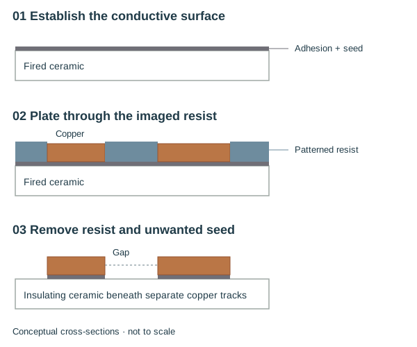
A fired ceramic surface is cleaned and prepared for a thin adhesion and conductive seed system. The adhesion layer anchors the metal to the ceramic; the seed provides the electrical path needed for electroplating.
Photoimaging defines the circuit pattern in resist. Copper is deposited in the exposed areas to build the tracks and pads, after which the resist and unwanted seed metal are removed. The result is an electrically separated pattern on the insulating ceramic, with copper build and feature geometry controlled as one process.
This route suits compact pad arrangements and fine interconnections on component carriers and optoelectronic submounts. The ceramic supplies insulation and heat conduction beneath the metal; the finished pad surface provides the connection to the component.
BONDED COPPER CIRCUITS
DBC and AMB form the interface before circuit etching
Both routes begin with copper sheet joined to ceramic. Circuit imaging and etching then remove unwanted copper, leaving pads and current-carrying areas. As copper thickness increases, lateral etching and conductor-edge shape become part of the spacing and dimensional design.
Direct bonded copper · DBC
A controlled copper–oxygen reaction forms the bond between copper and an appropriate ceramic surface at high temperature. The ceramic surface preparation and bonding cycle establish the interface; subsequent etching defines the circuit.
DBC is an established structure for power substrates requiring substantial copper areas, electrical insulation and a heat path through the ceramic.
Active metal brazing · AMB
An active braze layer joins copper to ceramic. Active elements react at the ceramic surface, enabling the metal-to-ceramic bond. This added joining layer distinguishes AMB from direct copper bonding.
Silicon nitride with AMB is a useful power-module construction where ceramic toughness and thermal-cycle performance are important. The braze interface, copper pattern and substrate act as one mechanical system.
Printed and thin-film circuits
Thick-film fabrication prints compatible pastes onto fired ceramic, dries them and fires them to form conductors, resistors or dielectric layers. Thin-film fabrication instead deposits thin metal or resistive layers and patterns them for the intended connections. Film composition, surface condition and the required circuit features determine the suitable route.
Co-fired multilayers
LTCC and HTCC start with unfired ceramic sheets. Conductors and via connections are formed before the sheets are stacked, laminated and fired together. Shrinkage and the compatible conductor system are part of the multilayer design. These processes use dedicated ceramic and conductor formulations, with the firing system selected together. The result is an embedded ceramic interconnection structure, distinct from metallizing an already-fired plate.
BARE SUBSTRATES TO POPULATED CIRCUITS
Finished Ceramic Boards and Assembly
FLJ supplies ceramic circuits with the patterned conductors, connection surfaces and mechanical form needed for the next build stage. Fabrication can continue into component sourcing and assembly for a populated board or subassembly.
Specify the complete circuit construction
| Part of the product | Construction options |
|---|---|
| Substrate | Alumina, aluminum nitride or silicon nitride; thickness and outline matched to the circuit and mounting arrangement. |
| Conductors | Plated copper, bonded copper or a compatible film system; single- or double-sided patterns and interconnections where the construction supports them. |
| Connections | Solderable pads, wire-bond surfaces or contact areas, with the selected metal stack and finish. |
| Mechanical form | Individual boards or arrays; holes, slots and outlines formed for the ceramic and assembly format. |
| Delivery | Patterned bare ceramic, populated boards or subassemblies; prototype and production quantities. |
Pad surfaces and precision machining
A finish protects the conductor and establishes the component-connection surface. A nickel/gold stack on copper, for example, has different layer functions: nickel provides a barrier, while the gold surface protects the connection area. Soldering and wire bonding place different demands on that stack, its surface condition and deposition process. FLJ matches the PCB surface finish to the conductor and attachment method.
Laser processing and precision machining form the required outline, openings and separation features. Ceramic is hard and brittle, so edge quality, hole position and local support matter during machining and singulation. A mounting opening provides mechanical clearance; an electrical via additionally needs a defined conductive wall or fill and connections to the circuit faces. Their fabrication routes and inspection therefore differ. The finished outline accommodates mounting loads and the intended contact with a cooling surface.
Checks tied to the ceramic circuit
Dimensional and visual inspection cover the circuit pattern, pad geometry, substrate edges and finished outline. Electrical continuity and isolation checks verify the connections; insulation and interface evaluations follow the selected construction and application. Metal adhesion and joint integrity concern the interface itself, beyond whether a track initially conducts.
Assembly on the actual substrate
SMT assembly connects solder-paste printing, placement and reflow for surface-mount ceramic boards. Board-temperature measurements establish a profile for the real substrate, copper and component loading. Fixturing supports the ceramic through printing, handling and separation, while the chosen pad finish and solder system define the connection.
Send the circuit drawing or manufacturing files, substrate preference and quantity to request a ceramic PCB quotation. For assembly, include the BOM and component placement data so fabrication and the populated-board supply can be quoted together.