


What does “heavy-copper PCB” mean?
Printed circuit boards come in many types. One of these types is the high-current PCB, also called a heavy-copper PCB. These boards have useful properties for applications that involve high current and changing temperatures. Heavy-copper PCBs can resist higher temperatures for longer times, they can handle higher current rates, and they provide stronger solder joints and connection points.
What is a high-current PCB?
A high-current PCB is a printed circuit board designed to support a higher critical current density than a standard PCB. A standard board may only support currents in the tens of amps. A high-current board can carry hundreds or even thousands of amps, and it can resist higher temperatures for long periods. The unique design of these PCBs uses thicker and heavier copper layers, and that gives the board stronger and more durable electrical and mechanical performance.
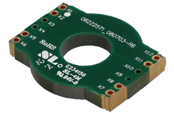
Heavy-copper PCBs typically contain more than 3 ounces of copper per square foot for carrying high current loads. Even when the total copper amount is less than 3 oz/ft², a board can still be classed as a heavy-copper PCB if the copper thickness on critical areas is more than 4 oz/ft². This large amount of copper is used when adding width to a trace is not possible or not the best option.
For example, on a DC motor PCB, the standard trace width needed to deliver the required power may be large, because designers must consider thermal constraints. Heavy-copper PCBs instead use thicker traces to achieve the same current carrying capacity while keeping trace width smaller. This helps save board space while maintaining thermal and electrical performance.
You will commonly find that the copper thickness used in Heavy-copper boards ranges from about 105 µm to 400 µm. In addition to higher copper thickness, these boards are able to dissipate heat at high temperature while offering stronger electrical connections. This thermal management helps heavy-copper PCBs avoid thermal stress and failure under heavy load.
Advantages of thick copper in PCB design
Thermal management is more important now than ever, because electronic equipment runs in harsher environments and at higher currents. Heavy-copper PCBs (for example, with internal and/or external copper conductors in the range 5 oz/ft² to 19 oz/ft², and sometimes defined as over 4 oz/ft²) help conduct heat away from components. This property can greatly reduce failures caused by overheating.
Proizvođači PCB-a use heavy copper to create robust conductor platforms. The resulting boards offer better conductivity and greater resistance to thermal stress. These boards can also achieve the same current capacity in a smaller area because a single layer can carry more copper weight or because multiple copper weights are placed on the same layer.
Key benefits of thick copper in PCBs include:
Reduced thermal strain on components and the board.
Improved current carrying capability.
Ability to survive repeated thermal cycling without damage.
Smaller finished board size in some designs, because copper stacking reduces the need for multiple layers.
Who benefits from heavy-copper PCBs?
Industries that gain clear benefits from heavy copper include:
Military and defense.
Automotive.
Solar panel systems (PV inverters and related equipment).
Welding equipment manufacturers.
Industrial control equipment.
These industries often need PCBs that can handle large heat output and that deliver reliable power distribution. Heavy-copper plated through holes are particularly good for moving heat to external heat sinks. Good power distribution is essential for high reliability, and heavy copper helps achieve it.

Heavy copper is not new. The method has been in use for many years to meet demanding military and defense requirements, such as weapon control systems. Now, mainstream electronics manufacturers also ask for better heat removal. Heavy copper has therefore become more common in non-military applications too.
How heavy copper is made and used
Heavy copper PCBs are usually made by a combination of electroplating i etching processes. The goal is to increase the copper thickness not just on flat traces but also on via sidewalls i plated holes. If a board is exposed to many production cycles, plated holes can wear or weaken. Adding heavy copper strengthens those plated holes and improves reliability.
A heavy-copper board lets you combine high-current or high-power zones and control or signal circuits on the same board. This avoids the need for separate power boards or bulky external wiring in some systems.
PHILIFAST works with customers to confirm and understand their needs. We match heavy copper manufacturing processes to those needs. For example, it is important to know the component types, how many layers are required, and what materials must be used. PHILIFAST can give a quote and explain the pros and cons of using heavy copper. Advances in technology have allowed processes that use both electroplating and edge milling or grinding to reach required copper thickness and flatness.
Copper thickness values used in heavy-copper PCBs
In practice, you will find the following:
Typical heavy copper thickness values fall in the range 105 µm to 400 µm.
Heavy copper is commonly described in ounces per square foot ili ounces per square foot (oz/ft²), or in the PCB industry more commonly as oz per square foot or oz per ft², though many suppliers use oz per square foot or convert to µm.
Standard copper weights like 1 unca correspond roughly to 34–35 µm of copper thickness for a single side, but the finished thickness depends on plating, surface finish, and lamination.
When vias and through-holes are plated and then thickened, both the hole copper and the surface copper may increase unless special steps are taken to control plating only in the drilled hole.
Board thickness and copper weight — impact on PCB design and manufacturing
When you cut boards from raw material, two main concerns are board thickness i copper weight. For raw board thicknesses above 0.8 mm, a standard set of thicknesses is commonly used: 1.0 mm, 1.2 mm, 1.6 mm, 2.0 mm, and 3.2 mm. For thicknesses below 0.8 mm, these are not considered the standard series. Thin board thicknesses are often customized. Common thin core thickness values used for inner layers include: 0.1 mm, 0.15 mm, 0.2 mm, 0.3 mm, 0.4 mm, and 0.6 mm. These thin core materials are mainly used as inner layers of multilayer PCBs.
When you design the outer layer and choose a finished board thickness, you must account for additional thickness added during production. These include:
Electroplated copper thickness added during via and hole plating.
Solder mask thickness.
Surface finish thickness (for example, hot-air solder leveling, ENIG gold plating, or other finishes).
Silk screen and carbon ink thickness.
In practice, a bare finished board will be thicker by about 0.05–0.1 mm than the core raw material because of these additions. Boards with tin plating typically show a larger final thickness increase, around 0.075–0.15 mm.
For example:
If your finished board requirement is 2.0 mm, and you choose 2.0 mm raw core material at the cutting stage, the final finished board will usually end up between 2.1 mm and 2.3 mm after fabrication tolerances and processing.
If your design absolutely requires the finished board to be no more than 2.0 mm, you should request a nonstandard raw board of 1.9 mm for fabrication. In that case, the fabricator must order nonstandard material from a raw material supplier, which will typically extend the delivery lead time.
For inner layer construction, you can adjust the final laminated thickness by choosing different prepreg thicknesses and by changing the layer stackup. The core choice is flexible. For example, to reach a 1.6 mm final thickness, you could choose a 1.2 mm core or a 1.0 mm core combined with suitable prepreg layers, as long as the final lamination keeps the finished thickness in the acceptable range.
Board thickness tolerance — what to expect
PCB designers must consider the finished board thickness tolerance along with product assembly tolerances. The main contributors to final thickness variance are:
Raw material tolerance from the board supplier.
Lamination process tolerance when multiple layers and prepregs are pressed together.
Extra thickness from outer layer copper and plating.
Typical raw material thickness tolerances often quoted for common panels are:
For 0.8–1.0 mm: ±0,1 mm.
For 1.2–1.6 mm: ±0.13 mm.
For 2.0 mm: ±0.18 mm.
For 3.0 mm: ±0.23 mm.
Lamination tolerance depends on the number of layers and the total thickness. It is commonly controlled to within ±(0.05–0.1) mm. Boards that include edge connectors or card edge contacts (like a printed card edge for a connector) need careful selection of thickness and tolerance to match connector specifications.
Surface copper thickness and plating standards
Via copper and plated hole copper are formed by chemical deposition followed by electroplating. If you increase plated hole thickness, surface copper thickness will often increase as well unless you take special control measures.
According to IPC-A-600G standard, the minimum copper plating thickness for plated holes is:
For Class 1 and Class 2 workmanship: 20 µm.
For Class 3 workmanship: 25 µm.
When you specify a copper weight of 1 unca, remember that 1 unca typically corresponds to a minimum raw foil thickness in certain systems, and finished thickness after plating can be higher. For example, if the raw foil option yields a minimum of 15.4 µm for a nominal 1 oz material in some manufacturing specifications, after allowing 2–3 µm of possible tolerance loss, the minimum might reach 33.4 µm in practice. If you choose a higher raw material or plating target, the finished copper thickness can reach 47.9 µm or more depending on the manufacturing route. Other copper thickness values follow similar calculation rules.
How to choose PCB thickness — what is standard?
PCB blanks (raw panels) do not have a single fixed global thickness. However, market convention and demand make certain thicknesses standard. You can get greater finished board thickness by stacking multiple prepregs and cores.
Common standard finished board thicknesses are:
0.031 in (0.78 mm).
0.062 in (1.57 mm).
0.093 in (2.36 mm).
The most common finished thickness in general electronics is 1.57 mm ili 0.062 in. But users and specific applications determine what thickness is standard for a product line. In early days, plywood was used as a substrate and boards were thicker. Over time, better options like epoxy glass (FR-4) became standard and allowed more control over finished thickness.
Factors that affect PCB thickness and copper weight
When planning board thickness and copper weight, consider these design and manufacturing factors:
Major cost drivers: board size and number of layers largely determine cost.
PCB complexity: layer count and number of vias affect both thickness and cost.
Materials used: choose materials based on operating speed, operating frequency, and maximum operating temperature.
Operating environment: whether the board must withstand high temperature, humidity, or mechanical stress will affect thickness choice.
Manufacturing factors: hole sizes and counts, copper weight, and surface finish options influence board thickness and final outcome.
Panelization method, gap between boards, and trace geometry: these affect routing, manufacturability, and final dimensions.
How to specify PCB copper thickness and trace width
You can use a trace width calculator to specify the copper thickness and trace width needed for a certain current. The tool works like a normal calculator: you input the current, allowable temperature rise, copper weight, PCB thickness, and other specs, and the calculator returns the required trace width and copper thickness. Many calculators provide precision down to 0.01 mm for accurate results. If your application requires the finished thickness to stay below a given limit, plan accordingly and adjust the stackup.
Things to remember when choosing PCB thickness
When you decide on board thickness to get better durability and performance, keep these specs and factors in mind:
Weight of the finished board.
Flexibility or rigidity required.
Impedance matching needs for high-speed signals.
Component height and space on the board.
Compatibility with the rest of the mechanical design.
Overall design rules and layout constraints.
What about custom board thickness?
Raw panels and sheets for PCB manufacturing are widely available. Many customization options exist so manufacturers can meet specific specs. You can choose thickness from 0.2 mm to 6.3 mm in 0.01 mm increments in many shops. The steps usually are:
Decide the common core/prepreg thicknesses you want to use.
Match them with copper foil, plated copper, and solder mask to reach the finished thickness.
Points to remember when ordering custom thickness:
Turnaround time: uncommon thicknesses require nonstandard material and so lead times increase. This affects delivery schedules and development time.
CM equipment capability: choose a contract manufacturer (CM) that has the right equipment. If the CM cannot manufacture your desired thickness, you may need to compromise and change some design choices.
Additional cost: custom specs cause higher production cost. Special materials, strict tolerances, and extra process steps all add cost.
Using custom thickness can improve the product’s performance and unique function. But multi-layer and custom boards come with extra handling, process steps, and material costs. That can make multilayer custom boards expensive.
Having a reliable manufacturing partner helps reach the desired thickness smoothly. The usual first step is to pick standard core/prepreg thickness values and then combine them with plated copper and copper foil and the chosen solder mask and surface finish.
PHILIFAST services and what we offer
At PHILIFAST, we meet customer needs with high-quality and accurate prototypes. We can support both standard and custom requirements and we pay attention to design intent. Highlights of our custom PCB manufacturing services include:
Accurate quotes within 24 hours.
Turnkey process completed in three days or less for many standard prototypes.
Shortened procurement time through supplier coordination.
Focused quality control and certification as required.
High PCB quality and automated optical inspection (AOI) in production.
If you need PCB manufacturing, PHILIFAST can offer prototypes and production services. We check customer requirements, discuss layer counts, material selections, copper weight, and other critical parameters. We also explain the pros and cons of heavy copper and how it will affect board cost, weight, and manufacturability.
Short technical summary and recommendations
Thick-copper PCBs are meant for high current and high thermal demand applications.
They use much thicker copper, commonly measured in oz/ft² or µm. Typical thick-copper values lie between 105 µm and 400 µm.
Heavy copper improves current carrying capacity and heat dissipation. It reduces thermal strain and can allow smaller board layouts for the same power.
Heavy copper is commonly applied by electroplating. It also strengthens plated holes and via sidewalls.
Designers must plan for additional thickness caused by plating, solder mask, and surface finish. Finished thickness is not the same as raw core thickness. Consider raw material tolerance and lamination tolerance.
Standard finished board thicknesses include 0.78 mm (0.031 in), 1.57 mm (0.062 in), i 2.36 mm (0.093 in), with 1.57 mm being the most common in general electronics. Custom boards can range from 0.2 mm to 6.3 mm.
When you design, consider cost drivers (size and layers), complexity (vias and layers), materials (speed, frequency, max temperature), and the operating environment.