
HIGH-CURRENT CIRCUITS · CUSTOM FABRICATION
Heavy Copper
PCB Manufacturing
More conductor cross-section.
Power and control on one board.
FLJ manufactures heavy copper PCBs for power conversion, motor drives and energy systems. Choose double-sided or multilayer constructions with finished outer copper up to 8 oz and inner copper up to 6 oz, supplied as bare boards or assembled circuits.
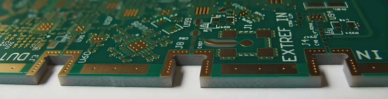
THE CONDUCTOR IS PART OF THE CONSTRUCTION
Heavy Copper PCB Capabilities and Construction Options
Heavy copper circuits use thicker copper tracks and planes to enlarge the conductive cross-section. Commonly described from around 3 oz upward, these boards put more metal into the electrical circuit. A copper core PCB instead uses a copper base as part of its heat-spreading structure.
| Copper weight | Approx. thickness | Minimum line / space | Layer position |
|---|---|---|---|
| 3 oz | 105 µm | 7 / 7 mil | Inner or outer |
| 4 oz | 140 µm | 12 / 12 mil | Inner or outer |
| 6 oz | 210 µm | 20 / 20 mil | Inner or outer |
| 8 oz | 280 µm | 28 / 28 mil | Outer |
Nominal thickness uses approximately 35 µm per oz/ft². These are construction-dependent fabrication references, not simultaneous limits or current ratings. Starting foil, finished circuit copper and plated-hole wall copper are separate specifications. The wider PCB manufacturing capabilities page covers other process ranges.
Power copper on the outer faces
Double-sided boards place the heavier copper directly at the component and connector surfaces. Broad current paths, power-device pads and connection lands share the outer-layer geometry. Copper thickness and feature spacing shape the available component escape and routing area.
Thick inner copper with finer outer routing
A multilayer construction can carry power on heavier inner layers while retaining finer outer connections for control components. This preserves routing and escape space at the component face. Pads and plated barrels feed the inner power paths, with their conductive sections developed alongside the heavier planes.
The inner copper still occupies thickness and needs resin around its etched features. Copper allocation, insulating buildup and the interlayer connections therefore form one construction.
Illustrative allocations only; layer thicknesses are not to scale and these sketches are not released stackups.
FOLLOW THE COMPLETE ELECTRICAL PATH
Current Capacity, Resistance and Thermal Paths
A thicker conductor provides more cross-sectional area within the same routing width. For a fixed length and copper temperature, increasing that area reduces resistance, voltage drop and resistive heating at a given current.
Resistivity × length, divided by conductor width × thickness.
Heating depends on current as well as the resistance of the path.
Copper weight is one input
At the same width, length and temperature, doubling the conductor thickness approximately halves its DC resistance. That comparison explains the value of heavier copper; allowable current also depends on how the board sheds heat. Layer position, nearby planes, laminate, airflow, ambient temperature and component heat all influence the temperature rise.
A continuous load and a short current pulse impose different thermal conditions. Current capability is established for the actual geometry and operating conditions, with temperature measurements taken at identified locations.
Include the narrow connections
A wide copper area may still feed a smaller pad neck, thermal-relief spoke or plated through-hole. These transitions are part of the same current path. Within a thin-walled plated hole, the conductive cross-section is approximately the barrel circumference multiplied by the copper-wall thickness.
Via count, finished diameter, wall copper and the connection to each plane affect the interlayer route. Specifying 6 oz on a circuit layer does not specify 6 oz on the hole wall. A pad-surface temperature measurement also describes that surface, rather than directly measuring the hidden barrel.
The finished copper dimensions and their transitions belong to one electrical and thermal construction.
FORM THE COPPER. FILL THE GAPS. CONNECT THE LAYERS.
Heavy Copper PCB Manufacturing
FLJ combines copper patterning, multilayer lamination, hole metallization and surface protection to produce the specified power circuit. Thick copper brings distinct geometry into these operations: taller conductor edges, deeper spaces between tracks and substantial copper at component connections.
Copper forming and etch compensation
The fabrication route starts with selected copper-clad material. Imaging defines the features; etching removes unwanted metal, while plating adds copper where the chosen process requires it. Heavy starting foil and plated copper builds place different demands on pattern formation.
Removing a deeper copper section increases the importance of solution exchange and lateral etching. Compensation in the manufacturing image accounts for the resulting conductor shape. Finished width, separation and sidewall geometry are checked together with copper thickness, keeping the circuit within the selected line-and-space range.
Plated holes and interlayer connections
Drilling establishes the holes through the laminated board. Hole preparation removes machining residues and exposes the interconnection surfaces. A conductive layer on the prepared wall enables copper deposition to build the plated barrel, linking outer pads and selected inner layers.
The wall-copper specification remains independent of the circuit-layer weight. Cross-section inspection can examine the barrel copper, inner-layer junctions and associated features. Hole and pad geometry also connect the electrical path to power connectors and through-hole components.
Lamination around thick inner copper
Etching a thick inner layer leaves deep spaces around its tracks and planes. During lamination, prepreg resin fills that copper-free volume and bonds the layers, while the buildup maintains insulation between neighboring conductors and copper faces. A sparse pattern and a densely coppered region present different fill volumes, even when their nominal copper weight is identical.
FLJ matches the prepreg resin and buildup to the pattern distribution and finished stack thickness. Cure and pressure follow the selected material system. The result is a bonded insulating structure around the tall copper features, rather than an unfilled step between layers.
Layer alignment holds pads and holes in the intended relationship. The board’s thermal exposure also influences the laminate choice; high-Tg materials provide a related option for the fabrication and assembly conditions.
POWER CIRCUITS IN WORKING ELECTRONICS
Applications in Power Electronics and PCB Assembly
Heavy copper serves circuits that distribute or convert substantial current. The layer arrangement connects that power function to the control electronics, mounting points and component interfaces of the finished product.
Motor drives and inverters
DC-link distribution and switching-stage connections link the supply to the power devices. Heavier copper provides conductor area for these paths, while finer outer routing can connect gate-drive, sensing and control components. Interlayer transitions connect the circuit to its device pads and terminals.
Industrial power conversion
Rectifiers, DC/DC converters and power-supply output stages use substantial copper around switching components, transformers and output connectors. Planar transformer windings are another application in which conductor cross-section, interlayer insulation and the winding arrangement are developed together.
Charging and energy systems
Charging converters and battery-system power distribution combine higher-current connections with monitoring and protection circuits. The board brings power routing, connection pads and sensing interfaces into a common assembly, with copper allocation suited to those different functions.
From fabricated power board to assembly
FLJ supplies prototypes and production boards, with component sourcing and PCB assembly available around the fabrication. Surface-mount control parts, power semiconductors and through-hole connectors can be combined in the populated build.
Heavier copper changes how heat reaches a joint during soldering. SMT printing, placement and reflow use the board’s measured thermal response to establish the soldering profile. Inspection and the selected functional tests address the assembled product.
Quote the board you need built
Send your fabrication files, copper allocation and quantity. Include the BOM and placement data for an assembled-board quotation.
Discuss a Heavy Copper Build