


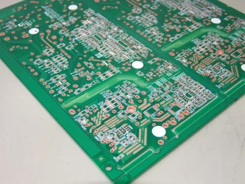
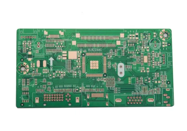
OSP is a surface finish for the copper foil on printed circuit boards (PCBs). It meets the RoHS directive. In simple terms, OSP is a thin organic film that is grown on a clean, bare copper surface by a chemical process. This film protects the copper from oxidation, heat shock, and humidity. It keeps the copper from rusting or sulfiding in normal conditions. At the same time, the film must be easy to remove quickly by flux during high-temperature soldering. That way the clean copper underneath can bond with molten solder fast and form a strong solder joint.
As electronic products become lighter, thinner, shorter, smaller and more functional, circuit boards move toward higher precision, thinner profiles, more layers, and smaller holes. SMT has developed fast. SMT uses high-density thin boards in devices such as IC cards, mobile phones, laptops, and tuners. Hot air solder leveling (HASL) then becomes less suitable for these needs.
At the same time, Sn-Pb solders used in HASL are not green. After the EU RoHS directive started on July 1, 2006, the industry needed lead-free alternatives for PCB surface finish. The common choices are OSP, ENIG (electroless nickel immersion gold), immersion silver, and immersion tin.
OSP Process Steps
Typical OSP process flow:
Degreasing (de-oiling) →
Double rinse with water →
Micro-etch →
Double rinse with water →
Acid wash →
DI water rinse →
Film formation and air dry →
DI water rinse →
Final drying
Below are details for the key steps and why they matter.
1. Degreasing
Good degreasing directly affects film quality. If degreasing is bad, film thickness will be uneven. To keep degreasing stable, control the chemical concentration in the cleaner within the process range. Also check degreasing performance often. If degreasing is poor, change the cleaner in time.
2. Micro-etch
Micro-etch makes the copper surface slightly rough. This helps the film bond. The micro-etch thickness affects the film formation rate. To get a stable film thickness, keep the micro-etch depth stable. Usually keeping it around 1.0–1.5 μm is appropriate. You can measure the micro-etch rate before each shift, then set the micro-etch time by that rate.
3. Film formation
Before film formation, rinse with DI water to avoid contaminating the film solution. After film formation, rinse with DI water again. Keep the rinse water pH between 4.0 and 7.0 to prevent the film layer from being polluted or damaged. Controlling the OSP film thickness is the key. If the film is too thin, it has poor heat shock resistance. During reflow, the film may not survive high temperatures (about 190–200 °C). Then soldering performance drops. On the assembly line, the film must be easy for flux to dissolve. Otherwise soldering will suffer. A common film thickness target is 0.2–0.5 μm.
Notes on OSP film
OSP films are very thin and can be scratched or rubbed off easily. Handle boards carefully in production and transport. Also, after many high-temperature soldering cycles, the OSP film on unused pads can discolor or crack. That affects solderability and reliability.
PCB Production Requirements for OSP Surface Finish
Below are production and handling rules to keep OSP boards reliable.
A. General production and storage rules
PCBs with OSP should arrive in vacuum packaging. Include a desiccant and a humidity indicator card. During transit and storage, place isolation paper between boards to prevent friction damage to OSP.
Do not expose boards to direct sunlight. Keep a proper warehouse environment. Relative humidity (RH): 30–70%. Temperature: 15–30 °C. Storage life should be less than 6 months.
When unsealing the board at the SMT station, check vacuum packaging, desiccant, and humidity card. If they fail, return the boards to the PCB maker for rework before use. Put the board onto the line within 8 hours after opening. Do not open many packs at once. Follow the rule “open as needed, produce as needed.” Long exposure causes batch soldering defects.
After stencil printing, pass the boards into the oven quickly. Do not let them sit. The maximum wait is 1 hour. Solder paste flux can strongly corrode the OSP film.
Keep the workshop environment steady. RH 40–60%. Temperature 18–27 °C.
During production, avoid touching the PCB surface with bare hands. Sweat and skin oils can cause oxidation.
If you do single-side SMT first, finish the second side SMT within 12 hours.
After SMT, finish DIP insertion as fast as possible, within 24 hours at most.
Do not bake damp OSP boards. High-temperature baking can discolor or degrade the OSP.
Unused boards that are overdue, damp, or cleaned after printing defects should be returned to the board maker for OSP rework. Do not rework the same board more than three times with OSP. After three reworks, scrap the board.
B. SMT stencil design rules for OSP boards
OSP boards are flat. That helps solder paste shape. But OSP pads cannot supply extra solder as HASL might. So enlarge stencil apertures slightly. This helps ensure solder covers the whole pad. When converting from HASL to OSP, redesign the stencil.
After enlarging the aperture, deal with solder ball, tombstoning, and exposed copper by changing the stencil hole shape to a “concave” design. This helps prevent solder ball formation.
If a component placement fails and the part is missing, make sure solder paste still covers the pad as much as possible.
To avoid exposed copper oxidation and reliability issues, consider printing solder paste on ICT test points, mounting screw holes, and exposed via pads (the backside can be wave soldered). Make sure to include these holes during stencil design.
C. Handling boards with bad solder paste print
Try to avoid printing errors. Cleaning will damage the OSP layer.
If a board has poor solder paste printing, do not soak or wash OSP boards with high-volatility solvents. Because the OSP film is easy to be eaten by organic solvents, use a non-woven cloth soaked in 75% ethanol to wipe off the paste. Then use an air blower to dry. Do not use isopropyl alcohol (IPA) to clean. Do not use a scraping knife to remove paste.
After cleaning a printing defect, finish the SMT work on that side within 1 hour.
For large batches of printing defects (for example 20 pieces or more), return them to the PCB maker for centralized rework.
What are the features of OSP in SMT assembly?
OSP boards need strict storage and handling. From the time you open vacuum pack to the first reflow or to the time after the first reflow, the stay time must be controlled strictly. Otherwise the second reflow quality will be affected. After one reflow cycle, the organic protective film on the PCB surface is usually destroyed and the board loses oxidation protection. Then second reflow is harder. Also OSP surface finish tends to have poorer solder paste wetting than some other finishes. Solder joints can expose copper and reliability can fall. The solder appearance may not meet IPC Class 3 standard easily. Many products that use pin-in-paste (PIP) are not good matches for OSP.
But OSP boards are flat and planar. Board manufacturing is stable and cost is low. Compared to others, OSP has clear advantages. So many companies still prefer OSP finish.
OSP Process Advantages
Low cost for SMT assembly.
High solder joint strength.
Good solderability when handled correctly.
Flat surface suitable for high-density pad design.
Compatible with mixed surface finishes (selective ENIG, for example).
Easy to rework.
OSP Process Disadvantages
Higher contact resistance. This can affect electrical testing.
Not good for through-hole soldering by line soldering.
Poor thermal stability and process robustness. After one high-temperature reflow, there is usually no more oxidation protection. The process window is short. All SMT steps after the first soldering should be finished within 24 hours.
Not corrosion resistant.
High demand on printing accuracy. Cleaning will damage OSP film (alcohols and acids can degrade OSP).
Poor solder-through performance for wave soldering holes.
Practical tips for using OSP boards on an assembly line
Always get OSP boards in vacuum packs with desiccant and a humidity card. Open one pack at a time. Use boards quickly.
Avoid touching exposed pads. Use gloves or tweezers when you must.
Keep the assembly environment stable: RH 40–60%, temp 18–27 °C.
Do not leave boards printed for more than one hour before reflow.
Keep time between first reflow and subsequent process steps short. Aim to finish all SMT within 24 hours after first reflow. Store reflowed boards in a dry cabinet if delay is unavoidable, and follow your PCB supplier’s guidance.
If you need to clean paste defects, use 75% ethanol on a non-woven cloth. Wipe gently. Dry with air. Do not soak. Do not use IPA or harsh solvents. Do not scrape with a blade.
Design stencils with slightly larger apertures for OSP pads. Consider concave aperture shapes to reduce solder ball issues.
For exposed test points and screw holes, consider printing solder paste to protect the copper if the design allows.
When to choose OSP
Choose OSP when:
You need a low-cost finish for high-density SMT boards.
You need a flat surface for fine pitch components.
Your assembly flow can control storage and timing strictly.
You accept the limits on thermal cycles and wave soldering.
Do not choose OSP when:
You need many high-temp cycles, or many wave-soldering steps.
You need long-term shelf life on exposed pads in the field without protection.
Your product must pass strict IPC Class 3 visual or solderability requirements without special controls.
Final notes on reliability and rework
OSP is reliable when handled right. The main risks are scratches, long exposure, long waits after opening, and repeated high-temp soldering. For mass production, set clear rules in the shop: one pack open at a time, use within hours, limit reflow cycles, and return suspect boards for rework. For rework at the PCB maker, track OSP rework counts. Do not rework the same board with OSP more than three times. After that, scrap the board.
About Philifast
Philifast offers PCB and PCBA services with OSP surface finish. We know OSP needs careful handling. We can supply boards in vacuum packs with desiccant and humidity cards. We help design stencils for OSP and give handling guidance so you get higher first-pass yield. If you need OSP boards with stable quality, fast lead times, and practical assembly support, Philifast can help. Contact us and we will work with your assembly line requirements.