
Organic solderability preservative
OSP PCB Manufacturing
Thin-film copper protection for fine-pitch assembly and economical PCB production.
FLJ manufactures OSP-finished printed circuit boards from prototypes to production batches. The organic film protects exposed copper soldering lands until assembly, with PCB fabrication and SMT assembly available through the same supply route.
Why choose OSP?
OSP Advantages and Applications
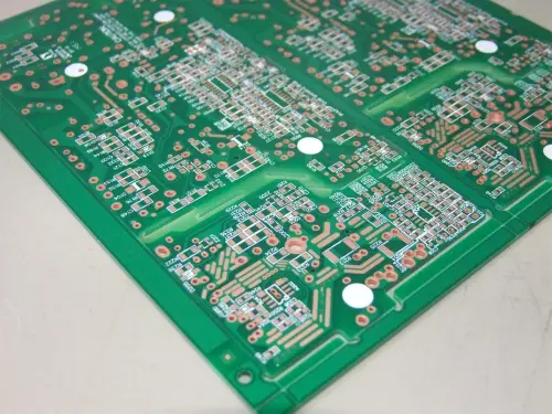
Exposed copper can oxidize before components are soldered, making reliable wetting more difficult. OSP limits that oxidation with a very thin organic film over the soldering lands, preserving a copper surface ready for the planned assembly.
A Flat Finish for Fine-Pitch SMT
OSP adds little build-up to the copper pads. A typical film is about 0.2–0.5 µm thick, depending on the formulation and process. This is useful for fine-pitch layouts where pad topography matters to solder-paste printing and component attachment.
Cost-Effective Copper Protection
The treatment protects soldering copper without depositing a nickel-and-gold stack. It offers an economical finishing route for production boards whose exposed lands are intended for solder joints.
A Lead-Free Surface Finish
The organic coating contains no lead-bearing solder layer. An appropriate OSP formulation can support lead-free assembly, with the finish and soldering sequence selected together.
From Protected Copper to a Solder Joint
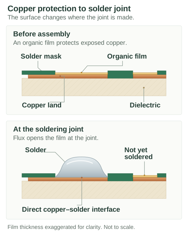
The film protects the copper during the interval between fabrication and soldering. At the joint, flux and the heating process open that protection so molten solder can wet the copper beneath it. Copper preservation before assembly and copper–solder contact during joining are the two parts of the same finishing task.
For batch production, FLJ can supply the finished boards or carry them into SMT assembly, including paste printing, placement and reflow. Coordinating board delivery, pack opening and assembly helps retain the protected surface until it is used.
Double-Sided and Sequential Assembly
In a double-sided build, second-side lands still need to accept solder after the first heating cycle. A suitable OSP formulation and assembly profile support that sequence; later wave or selective soldering also needs to account for the heat already experienced by the remaining lands.
Soldering Lands and Hard-Gold Contacts
Boards with edge connectors can combine OSP soldering areas with selective hard-gold fingers. The organic film preserves copper for joining, while the hard-gold regions provide the repeated-mating surface. FLJ supplies these region-specific finishes within the same board construction.
The coating chemistry
OSP Coating Types and Selection
OSP describes a family of organic copper-protection treatments. Modern formulations commonly use azole chemistry; the chosen product determines the protection and thermal performance needed for the assembly.
From Resin Protection to Azole-Based Films
Scroll to read all columns →
| Protection system | Copper-protection approach | Assembly consideration |
|---|---|---|
| Earlier rosin / resin treatments | Rosin, rosin-ester and resin-based films cover copper with an organic protective barrier. | These earlier approaches provide the background to organic copper protection. Their response to heating depends on the particular material and process. |
| Modern azole-based OSP | Azole compounds interact with the copper surface to form the protective film. Examples include benzotriazoles, imidazoles and benzimidazoles. | A suitable formulation preserves the soldering copper through the specified lead-free profile and any later soldering operations. |
Matching the Formulation to Assembly
The selected formulation provides the thermal capability needed by the build. Lead-free reflow exposes the film to the chosen temperature profile; second-side or later soldering also requires useful protection on the lands that remain unsoldered. A heat-resistant grade addresses those demands within the coating system. Its suitability follows the actual profile and sequence, rather than a fixed cycle count assigned to the chemistry family.
For boards requiring another surface function, the surface-finish selection also needs to account for soldering lands, contacts and any bonding areas.
From prepared copper to a protected surface
OSP PCB Manufacturing Process
FLJ prepares the exposed copper and forms the OSP finish after the circuitry and solder-mask pattern are in place. The following operations connect clean copper, selective film formation and protective packing. Pretreatment and intermediate rinses follow the selected chemical system.
Copper Cleaning
Cleaning removes oils, handling contamination and unwanted surface residues from the exposed copper. A consistently clean surface allows the following treatment to reach the lands uniformly.
Controlled Micro-Etching
Controlled micro-etching removes a small amount of surface copper and establishes the condition required by the coating system. This prepares the copper for consistent film formation across the intended features.
Pretreatment Rinsing
The prescribed rinse and pretreatment stages clear residues and prepare the copper for the OSP treatment. Intermediate rinsing controls carryover between process stages; its arrangement follows the selected chemistry.
OSP Film Formation
The treatment chemistry interacts selectively with the exposed copper to form the organic protection. Bath concentration, temperature and contact time control film formation. The resulting layer must protect copper before assembly and allow the soldering process to reach it at the joint.
Deionized-Water Rinsing
Deionized-water rinsing removes treatment carryover and unwanted residues before drying. This keeps the coated surface clean as it leaves the wet process.
Drying and Protective Packing
The treated boards are dried, examined and protectively packaged for delivery. Board separation limits rubbing against the soldering lands; the packing arrangement preserves the finished surface until the boards enter assembly.
Film Consistency and Solderability
Consistent film coverage protects the intended copper lands. Too little protection can expose copper to oxidation, while excessive film can be harder for the soldering process to open. Surface examination addresses contamination, damage and treatment consistency; film-thickness evaluation checks the coating amount for the selected system. Where the build requires it, solderability testing checks whether the surface wets under the intended conditions, including relevant prior heating.
Preserving the supplied finish
OSP PCB Storage and Soldering
The thin film is sensitive to contact, contamination and the board’s exposure history. Packaging and assembly handling preserve the copper surface that the soldering process will need to reach.
Scroll to read all columns →
| Board state | Surface exposure | Handling and assembly focus |
|---|---|---|
| Sealed boards | Storage and transport in protective packaging. | Maintain the specified storage conditions and packaging. Separate boards to limit rubbing of the soldering lands. |
| Opened production packs | Handling, ambient exposure and contact during production. | Use clean handling and coordinate printing and assembly so that opened boards do not wait unnecessarily. |
| After assembly heating | Soldered areas and remaining unsoldered lands have different surface histories. | Match subsequent soldering and any required moisture treatment to the formulation, thermal profile and actual board condition. |
A colour change after heating is an observation about the surface, rather than a complete solderability result. Storage duration, baking and repeat heating follow the selected coating and board requirements.
Fabricated boards or assembled PCBs
OSP PCB Manufacturing Capabilities and Supply
FLJ supplies OSP-finished boards for prototype and production orders, with assembly available for the same build. Specify the soldering areas, any selective contact finish and the planned assembly sequence with the fabrication requirements.
| Manufacturing item | Reference |
|---|---|
| Processing edge length | Single edge <500 mm |
| Minimum processing panel | 60 × 80 mm |
| PCB thickness | 0.3–3.0 mm |
| Finishing-route aspect ratio | 8:1 |
The panel dimensions describe surface processing; smaller finished boards can be panelized. The aspect ratio is an OSP finishing reference, separate from the drilling capability. Film thickness is specified for the selected coating system.
Quote Your OSP PCB Build
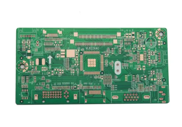
Send the board files, quantity and finish requirements. Include assembly needs and any areas requiring a different contact finish.