


Efficient, Accurate, and Standardized Service
- High-Difficulty PCB Reverse Engineering Service
- Guaranteed 100% Accuracy of PCB Files with 1mil Precision
- Expert in Laser Blind Via Boards
- Proficient in Rigid-Flex Boards, Differential and Serpentine Routing
Inženjering obrnutog dizajna štampanih pločica
Over 10 years of technical expertise, skilled in complex projects and advanced PCB reconstruction.
Chip Reverse Analysis
High decryption success rate with broad chip coverage, delivering reliable reverse engineering solutions.
OEM Manufacturing
2–44 layer high-quality PCB production with precise prototyping and professional processing services.
Philifast PCB Reverse Engineering Services
Advanced Technology
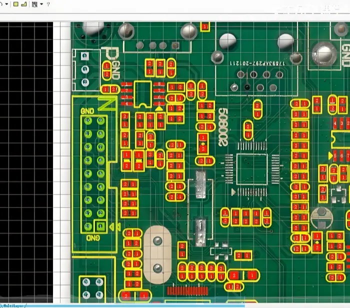
Philifast utilizes industry-leading PCB scanning technology, unique intelligent PCB reverse engineering software, and integrates years of circuit board expertise and practical experience. Combined with advanced EDA design tools, a professional engineering team, and refined manufacturing techniques, we can accurately clone single-layer, double-layer, and multilayer PCBs up to 32 layers.
Complex Design Expertise
We handle complex PCB designs involving blind and buried vias. Whether it’s a densely populated computer motherboard, graphics card, or gigabit network baseboard—Philifast guarantees 100% accuracy identical to the original.
Custom Redesign
Our professional modification team provides tailored PCB redesign services including component relocation, layout optimization, and circuit rerouting to meet your specific requirements.
Comprehensive Deliverables
We convert PCB samples into production-ready Gerber files and generate multiple design formats. Additional services include sample production, schematic recreation, BOM lists, and more.
Quality Assurance
With advanced testing equipment, we ensure high success rates, reduce redesign time and cost, and help customers maintain market leadership while providing valuable resources.
Ready to Get Started?
Contact Our Engineering Team
Advanced Technology
Philifast utilizes industry-leading PCB scanning technology, unique intelligent PCB reverse engineering software, and integrates years of circuit board expertise and practical experience. Combined with advanced EDA design tools, a professional engineering team, and refined manufacturing techniques, we can accurately clone single-layer, double-layer, and multilayer PCBs up to 32 layers.
Complex Design Expertise
We handle complex PCB designs involving blind and buried vias. Whether it’s a densely populated computer motherboard, graphics card, or gigabit network baseboard—Philifast guarantees 100% accuracy identical to the original.
Custom Redesign
Our professional modification team provides tailored PCB redesign services including component relocation, layout optimization, and circuit rerouting to meet your specific requirements.
Comprehensive Deliverables
We convert PCB samples into production-ready Gerber files and generate multiple design formats. Additional services include sample production, schematic recreation, BOM lists, and more.
Quality Assurance
With advanced testing equipment, we ensure high success rates, reduce redesign time and cost, and help customers maintain market leadership while providing valuable resources.
Ready to Get Started?
Contact Our Engineering Team6 Advantages of Choosing Us
1️⃣ Always Focused on Customer Needs
Meeting customer requirements is the foundation of our company. We’ve built a complete customer-centered management system, invested in R&D, and improved staff skills to ensure every client’s needs are met.
2️⃣ Tailored Technical Solutions
We provide customized electronic product design and development services, offering targeted solutions to all your technical challenges.
3️⃣ Professional Technical Team
Over 90% of our engineers have more than five years of experience. Our departments include PCB Design, Reverse R&D, Chip Decryption, and Disassembly, ensuring highly specialized service.
4️⃣ Rigorous Quality Assurance System
With years of industry experience, we’ve established a strict reverse engineering quality system to guarantee reliable and high-performance products.
5️⃣ Excellent After-Sales Support
Guided by the principle of “Service First,” we are committed to providing the best after-sales support across the entire industry.
6️⃣ One-Stop Design, Development & Manufacturing Service
Combining years of reverse engineering experience with advanced production and processing, we assist customers from concept to final product launch.
Advantages of PCB Reverse Engineering with Us
Free Evaluation Before Projects
- Check for encrypted programs
- Verify if there are polished or fake chip models
- Identify discontinued or otherwise unavailable components
Note: If any of the above issues cannot be resolved, it may affect the completeness of the project data.
Fast, Accurate, and Cost-Effective PCB Reverse Engineering
PCB reverse engineering costs are calculated based on the number of pads. Prices vary depending on the number of layers and specific requirements.
Typical turnaround times:
• Single- or double-layer boards: 1–2 days
• 8-layer boards: 5–7 days
More complex boards (many components, multiple layers, complex structures) are assessed individually based on the physical sample.
Our collaboration principle: "Create a win-win situation with our clients."
Strong Overall Capabilities
We provide a full range of services, including PCB reverse engineering, PCB design, prototype debugging, BGA soldering, component selection, IC procurement, high-precision PCB fabrication, and SMT assembly.
We can design products according to client requirements, including functional improvements and technical optimizations of existing products through secondary development.
With over 10 years of practical experience, we have carried out secondary development and prototyping for electronic products across industries, achieving a 100% success rate in PCB reverse engineering.
Free Evaluation Before Projects
- Check for encrypted programs
- Verify if there are polished or fake chip models
- Identify discontinued or otherwise unavailable components
Note: If any of the above issues cannot be resolved, it may affect the completeness of the project data.
- Check for encrypted programs
- Verify if there are polished or fake chip models
- Identify discontinued or otherwise unavailable components
Fast, Accurate, and Cost-Effective PCB Reverse Engineering
PCB reverse engineering costs are calculated based on the number of pads. Prices vary depending on the number of layers and specific requirements.
Typical turnaround times:
• Single- or double-layer boards: 1–2 days
• 8-layer boards: 5–7 days
More complex boards (many components, multiple layers, complex structures) are assessed individually based on the physical sample.
Our collaboration principle: "Create a win-win situation with our clients."
Strong Overall Capabilities
We provide a full range of services, including PCB reverse engineering, PCB design, prototype debugging, BGA soldering, component selection, IC procurement, high-precision PCB fabrication, and SMT assembly.
We can design products according to client requirements, including functional improvements and technical optimizations of existing products through secondary development.
With over 10 years of practical experience, we have carried out secondary development and prototyping for electronic products across industries, achieving a 100% success rate in PCB reverse engineering.
PCB Reverse Engineering Process
We produce the sample board in-house and deliver it for test/approval.
Customer opts to build their own prototype based on provided files.
Proceed directly to production or file delivery.
Purchase components according to BOM. (Prototype may be required)
Customer supplies the required test or operating environment for debugging.
Assemble and debug the prototype in the specified test environment.
Create the BOM for procurement and assembly.
Decide whether the original schematic is needed or must be reverse-engineered.
Reconstruct the circuit schematic from the sample board.