


Znáte to. Máte schéma, které funguje. Rozložení plošného spoje vypadá čistě. Možná se vám dokonce vrátil prototyp a blikal, startoval, měřil, vysílal. Skvělé.
Pak se objeví realita.
Nyní potřebujete deset desek. Nebo sto. Nebo jste právě dostali povolení k zahájení výroby skutečného produktu a najednou se otázky množí. Kdo obstarává součástky? Co se stane, když se nějaká součástka objedná? Potřebujete AOI, rentgen, funkční testování, konformní povlak? Zachytí montážní firma vaši chybu v otisku patky dříve, než umístí 500 špatných konektorů?
Právě na tomto skoku od prototypu k výrobě se mnoho projektů zadrhne. Ne proto, že by byl nápad špatný. Ale proto, že osazování desek plošných spojů je svébytné řemeslo, a když ho děláte “většinou správně”, skončíte s přepracováním, zpožděním a deskami, které se chovají v jednotlivých sériích jinak.
Pojďme si tedy říct, jak správně dělat PCBA. Co se mění mezi prototypem a výrobou. Co je třeba připravit. Co hledat u výrobního partnera. A jak udržet proces nudný, předvídatelný a opakovatelný. Upřímně řečeno, to je cíl.
Prototyp vs. výrobní PCBA není stejná hra
Běh prototypu odpouští.
Pokud stavíte 2 až 5 jednotek, můžete podivný díl umístit ručně. Můžete vyměnit alternativní hodnotu rezistoru. Signál můžete zapojit. Můžete přetavovat v troubě na opékání topinek a přesto poslat předváděcí jednotku investorovi.
Produkce vám to nedovolí. Produkce je o důslednosti.
“Fungující” prototyp neznamená, že máte automaticky vyrobitelný produkt. Výroba totiž přináší nová omezení:
- Dostupnost komponent se stává neustálým bojem.
- Výtěžnost montáže záležitosti. Dvouprocentní chybovost je u 5 desek nepříjemná, ale u 500 desek drahá.
- Testovací strategie záležitosti. Potřebujete způsob, jak rychle ověřit jednotky.
- Dokumentace se stává součástí produktu. Není volitelné.
- Kontrola kvality se stává systémem, ne člověkem, který zírá na tabuli.
Skutečná otázka tedy nezní “dokážeme ji sestavit”. Jde o to, “zda ji dokážeme sestavit stejným způsobem, pokaždé a ve velkém měřítku”.
Nudný kontrolní seznam, který zachrání váš projekt
Než odešlete soubory k montáži, ujistěte se, že na ně dokážete odpovědět bezchybně. Pokud to nedokážete, desky sice dostanete, ale zaplatíte za zmatek.
1) Je váš kusovník skutečně sestavitelný?
A Soupis materiálů, který funguje pro prototypování může být pro výrobu nepořádek.
Běžné problémy:
- Chybějící nebo nejasná čísla dílů výrobce.
- “Jakýkoli kondenzátor 10uF” bez jmenovitého napětí, obalu, dielektrika nebo tolerance.
- Zastaralé součástky, které jste převzali ze starého referenčního návrhu.
- Jednotlivé zdroje integrovaných obvodů s dlouhými dodacími lhůtami.
- Díly uvedené s interní přezdívkou místo skutečného objednatelného dílu.
Pro výrobu musí být kusovník jednoznačný. Až po balení, pokud na něm záleží. Pokud používáte drobné pasivy, opravdu na tom záleží.
Osvědčeným postupem je zahrnout:
- MPN
- Popis a klíčové specifikace
- Schválení náhradníci (alespoň pro pasivní)
- Množství na desku a celkové množství
- Poznámky jako “DNF” nebo “nenahrazovat” u kritických položek.
A ano, je to únavné. Ale je to levnější než zastavení výrobní linky, protože si někdo vyložil volbu kondenzátoru jinak, než jste očekávali.
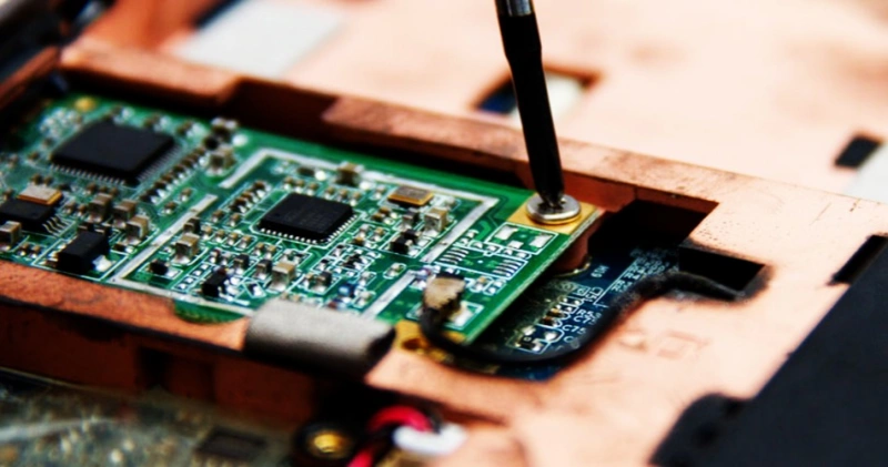
2) Jsou vaše otisky a označení polarity jednoznačné?
Zde se z malých chyb stávají velké účty.
Prototypové týmy se někdy spoléhají na kmenové znalosti. Pamatujete si, že stopa diody je zrcadlově obrácená, ale kompenzovali jste to v rozložení. Montér si to nepamatuje. Budou se řídit údaji ze silokarty a centroidu.
Proveďte rychlý průchod speciálně pro montáž:
- Indikátor Pinu 1 na integrovaných obvodech.
- Značení polarity na diodách, LED, elektrolytech, tantalech.
- Orientace konektoru je jasná.
- Fiduciály jsou přítomny a nejsou blokovány sítotiskem.
- Nádvoří a hlídání respektováno, zejména v blízkosti vysokých částí.
Pokud máte díly s jemnou roztečí, ujistěte se. otisk je správný a ověřený podle datasheetu., nikoliv zkopírované z náhodné knihovny. Všichni jsme to jednou udělali. Není to legrace.
3) Je vaše strategie šablony a lepidla pro desku správná?
Objem pájecí pasty je jedním z těch nudných detailů, které rozhodují o tom, zda bude vaše montáž probíhat hladce, nebo bolestivě.
Pokud používáte:
- Balení QFN, BGA nebo LGA
- Velké tepelné podložky
- Velmi malé pasivy 0402 nebo 0201
- Smíšená technologie s velkými konektory a malými integrovanými obvody
Pak možná budete potřebovat úpravy otvoru šablony. Redukce pasty na tepelných podložkách. Okenní vzory. Podobné věci.
Nejedná se o “nadměrné inženýrství”. Je to rozdíl mezi deskou, která projde přetavením, a deskou, která se překlene, plave nebo se stane hrobem.
4) Jaký je váš plán testování?
Pokud testujete pouze připojením kabelu a doufáte, že se spustí, je to pro pět jednotek v pořádku. Později se to rychle pokazí.
Výroba potřebuje opakovatelný a rychlý testovací proces. Dokonce i jednoduchý.
Mezi možnosti patří:
- Základní kontroly napájecích kolejnic.
- Ověřování hranic nebo programování.
- Funkční zkouška pomocí přípravku.
- Při testování v okruhu, pokud to objemy odůvodňují.
Minimálně definujte, co znamená “projít”. A jak dlouho by měl test trvat. Pokud je jediným způsobem testování patnáctiminutové šťourání člověka multimetrem, pocítíte to.
Co vlastně znamená “správně provedená montáž PCB”
V oblasti PCBA je spousta marketingu. Všichni říkají, že je to rychlé, kvalitní a levné. Všechno najednou.
V praxi to obvykle znamená, že máte partnera, který tyto oblasti zvládá bez problémů.
Spolehlivé zdroje, ne jen levné zdroje
Ve výrobě je shánění komponentů polovina práce.
Dobrý partner pro PCBA:
- Označte rizikové části. Dlouhé dodací lhůty, jediný zdroj, NRND.
- Navrhněte alternativy, které odpovídají vašim specifikacím.
- Před objednáním si ověřte typy balení a velikosti cívek.
- V případě potřeby používejte sledovatelné napájecí kanály.
Levný zdroj může být později drahý, pokud vede k padělkům, smíšeným datovým kódům nebo nekonzistentním dílům. Pokud se váš výrobek musí chovat předvídatelně, chcete předvídatelnost i v dodavatelském řetězci.
Kontrola procesu: pasta, umístění, přetavení, kontrola
Kvalita montáže není kouzelná. Je to proces.
Vyspělá montážní linka se stará o:
- Konzistence tisku pájecí pasty.
- Přesnost výběru a umístění.
- Profil přetavení přizpůsobený vaší desce.
- Správné zacházení se zařízeními citlivými na vlhkost.
- Úklid, pokud ho potřebujete.
- Kontrola AOI a rentgenové snímky skrytých spojů.
I když neobjednáváte tisíce kusů, platí stejná disciplína. Díky ní se udržuje vysoká výtěžnost.
Komunikace, která včas zachytí problémy
Zní to jemně, ale je to obrovské.
Nejlepší sestavy jsou ty, kde vám někdo před stavbou napíše krátký seznam otázek, jako např.:
- “Tento kondenzátor je uveden jako 10uF, ale bez jmenovitého napětí.”
- “R15 je v kusovníku označen jako DNF, ale má záznam v souboru umístění.”
- “U3 se zobrazuje jako QFN 4×4, ale půdorys vypadá 3×3.”
- “Vaše deska nemá žádné otvory pro nástroje. Chcete, abychom přidali panel?”
To není otravné. Je to druh tření, který zabraňuje katastrofám.
DFM není módní slovo, je to vaše pojistka
DFM, Design for Manufacturability, se často skloňuje. V jádru je to však jednoduché.
Je navržena tak, aby bylo možné desku sestavovat snadno, opakovaně a s vysokou výtěžností.
Několik detailů DFM, na kterých záleží více, než si lidé myslí:
- Rozestupy mezi díly, aby se trysky mohly správně umístit.
- Důsledná orientace polarizovaných dílů, aby se snadněji umísťovaly a kontrolovaly.
- Definice pájecí masky které odpovídají vaší technologii.
- Panelizace který podporuje stabilní zpracování. Zejména pro malé desky.
- Jasné referenční označení které nejsou schované pod díly nebo odříznuté.
A tady je upřímná pravda. DFM je často smyčka, nikoli jednorázový úkol.
Vytvoříte prototypy, zjistíte, co bylo bolestivé, upravíte design a pak jej uzamknete pro výrobu. To je normální. Je to zdravé.
NPI: nepříjemná střední fáze, kterou byste měli plánovat
Pokud přecházíte z prototypu do výroby, obvykle procházíte NPI, New Product Introduction.
NPI je mezistupeň, kdy už nejste hacker, ale také nejste zcela stabilní.
Tady byste měli udělat:
- Pilotní série, například 10 až 50 kusů.
- Validace procesu.
- Validace zkušebního přípravku.
- Ověření obalu.
- První kontrola článku.
- Kontrola revizí je dostatečně přísná, aby nikdo nevytvářel “Rev A, ale s tou jednou změnou, o které jsme mluvili”.
Není to nijak okouzlující, ale je to místo, kde si vybudujete jistotu, že se výroba nezmění v hašení požáru.
Jednoduchý pracovní postup, který udržuje věci v rozumné míře
Pokud chcete přímou cestu od prototypu k výrobě, je to dobrý základ.
Krok 1: Dokončení souborů návrhu
- Gerbers
- Vrtací soubory
- Poznámky ke skládání DPS, pokud je to relevantní
- Montážní výkresy
- Vybírání a umísťování souborů
- kusovník s náhradními díly
Krok 2: Přezkum DFM a DFA
- Přezkum výroby
- Recenze sestavy
Krok 3: Vytvoření prototypu nebo pilotního projektu
- Sestavte malou šarži
- Problémy se zachycením a opravy
Krok 4: Revize zámku a dokumentace
- Proces ECO
- Verzované výstupy
Krok 5: Výrobní sestavení
- Definovaná kontrola a zkouška
- Definované balení
- Sledovatelnost podle potřeby
Zní to samozřejmě. Je to tak. Ale “samozřejmost” je také to, co týmy vynechávají, když spěchají. Rozpis je pak později trestá.
Výběr partnera pro PCBA bez zbytečného přemýšlení
Nepotřebujete dokonalého výrobce. Potřebujete správného výrobce.
Na co bych se zaměřil, zejména pokud dodáváte skutečný produkt, a ne jen laboratorní desky:
- Nabízejí výroba i montáž desek plošných spojů, nebo to mohou čistě koordinovat?
- Mohou podporovat rychlé zatáčky když ji potřebujete?
- Pomohou s získávání komponentů, včetně náhradníků?
- Poskytují možnosti kontroly jako je AOI a rentgen v případě potřeby?
- Reagují na otázky a nemlčí, dokud nedorazí komise?
- Mohou vás podpořit i nad rámec montáže, například testování, balení a průběžný provoz?
Na kvalitě komunikace záleží téměř stejně jako na strojích. Většina problémů s PCBA totiž nespočívá v tom, že “stroj to špatně umístil”. Jsou to problémy s nepochopením. Špatný díl. Špatná orientace. Nejasné soubory. Zamlčené předpoklady.
Jak se k tomu staví společnost Philifast
Pokud hledáte partnera pro výrobu PCBA, který dokáže podpořit zakázkovou elektroniku od počátečních sestav až po sériovou výrobu, je to pro vás ta správná volba. Philifast přichází.
Zaměřují se na věci, na kterých obvykle záleží nejvíc, když se snažíte odeslat něco skutečného:
- Vysoce kvalitní osazení PCB
- Rychlé vyřízení když jsou termíny napjaté
- Spolehlivá výrobní podpora, ne jenom sestavení s volnýma rukama
- Nápověda pro celý proces, abyste nemuseli žonglovat s pěti dodavateli a doufat, že všichni budou vaše soubory interpretovat stejně.
Hledáte vysoce kvalitní služby v oblasti PCBA?Společnost Philifast je zde, aby podpořila váš projekt zakázkové elektroniky rychlým zpracováním, spolehlivou montáží a plnou výrobní podporou. Kontaktujte nás ještě dnes na adrese flj-pcb.com pro rychlou cenovou nabídku.
Závěrečné myšlenky
Dostat se od prototypu k výrobě neznamená najít továrnu a poslat Gerbery.
Jde o vytvoření opakovatelného procesu. Čisté kusovníky. Přehledná montážní data. Kontroly DFM. Plán testování, který nespoléhá na štěstí. A výrobního partnera, který včas komunikuje, zodpovědně zajišťuje zdroje a dokáže zajistit stálou kvalitu.
Pokud to uděláte, PCBA se stane nudným.
A nuda je přesně to, co chcete, když jde o váš produkt.
Často kladené otázky (FAQ)
Jaké jsou hlavní rozdíly mezi prototypovou a výrobní montáží DPS?
Osazování prototypů desek plošných spojů je šetrné a flexibilní, umožňuje ruční umísťování dílů, záměny a ruční přepracování. Výrobní montáž DPS vyžaduje konzistenci, vyrobitelnost, řízení dostupnosti součástek, optimalizaci výtěžnosti montáže, robustní testovací strategie, důkladnou dokumentaci a systematickou kontrolu kvality pro zajištění opakovatelných výsledků ve velkém měřítku.
Proč je pro výrobu PCBA klíčový dobře definovaný kusovník?
Jasný a jednoznačný kusovník je pro výrobu zásadní, protože zabraňuje zmatkům a zpožděním. Měl by obsahovat přesná čísla dílů výrobce (MPN), podrobné popisy s klíčovými specifikacemi, schválené alternativy, množství na desku a celkovou objednávku a poznámky typu ‘nenahrazovat’ u kritických komponent. Tato úroveň detailů zajišťuje, že díly jsou dodávány správně a konzistentně ve velkých výrobních sériích.
Jak mohu zajistit, aby mé otisky desek plošných spojů a označení polarity byly vhodné pro výrobu?
Abyste se vyhnuli nákladným chybám při montáži, ověřte, zda všechny otisky přesně odpovídají specifikacím v datasheetu. Jasně označte pin 1 na integrovaných obvodech, polaritu na diodách, diodách LED, elektrolytech, tantalech a zajistěte jednoznačnou orientaci konektorů. Uveďte pomocné značky, které jsou viditelné a nejsou zakryty sítotiskem. Respektujte nádvoří a ochranné prostory kolem vysokých součástek, abyste usnadnili jejich správné umístění.
Jaká hlediska je třeba brát v úvahu při návrhu šablony pájecí pasty pro výrobní PCBA?
Objem pájecí pasty zásadně ovlivňuje kvalitu montáže. U obalů, jako jsou QFN, BGA, LGA nebo desky s velkými tepelnými podložkami a velmi malými pasivy (0402 nebo 0201), mohou být nutné úpravy šablonových otvorů, jako je zmenšení pasty na tepelných podložkách nebo okenní vzory. Správný návrh šablony zabraňuje vzniku vad, jako je přemostění pájky, plovoucí součástky nebo tombstoning během přetavení.
Proč je strukturovaný testovací plán důležitý pro přechod od prototypu k výrobnímu PCBA?
Výroba vyžaduje rychlý a opakovatelný zkušební proces, který spolehlivě ověří každou jednotku. Na rozdíl od prototypů, kde může postačovat neformální testování, mohou plány výrobních testů zahrnovat kontrolu napájecích lišt, hraniční skenování nebo ověření programování, funkční testy pomocí přípravků nebo testování v obvodech, pokud to odůvodňují objemy. Definování jasných kritérií průchodnosti a doby trvání testů pomáhá udržet kvalitu a zároveň minimalizovat úzká místa.
Co znamená ‘správně provedená montáž desek plošných spojů’ kromě rychlé a levné výroby?
‘Správně provedená montáž desek plošných spojů’ znamená zavedení konzistentních procesů, které produkují spolehlivé desky šarži za šarží bez překvapení. Zahrnuje pečlivou přípravu včetně sestavitelných kusovníků, přesných otisků s jasným značením, optimalizovaných návrhů šablon pro nanášení pájecí pasty, komplexních testovacích strategií, důkladné integrace dokumentace do životního cyklu výrobku a systematické kontroly kvality - nikoli pouze marketingové sliby o rychlosti nebo nízkých nákladech.

