


Printed Circuit Boards (PCBs) are the foundation of modern electronics, from consumer gadgets to critical aerospace systems. As devices become more complex and compact, the margin for error in the manufacturing process shrinks to nearly zero. This is where a rigorous quality assurance strategy becomes paramount. Comprehensive PCB testing is not merely a final checkpoint; it’s a multi-stage, systematic process designed to validate design intent, ensure electrical integrity, and guarantee long-term reliability. A flawed circuit board can lead to costly recalls, catastrophic failures, and damaged brand reputations, making a robust testing ecosystem an indispensable investment.
The Imperative for Flawless Printed Circuit Boards
In an interconnected world, the performance of a single circuit board can impact entire systems. The demand for flawless PCBs is driven by consumer expectations for reliability and the stringent safety requirements of industries like automotive and medical. A single microscopic defect—a hairline crack in a copper trace or an imperfect solder joint—can compromise the function of the entire product. Effective PCB testing methods are the only way to systematically detect and eliminate these potential points of failure.
Understanding the Stakes: Costs of Defects and Importance of Reliability
The cost of a defect increases exponentially as it progresses through the manufacturing process. A design flaw caught on paper is inexpensive to fix. A defect on a bare board is more costly. A failure discovered after components are assembled (creating a PCBA) requires significant rework. Worst of all, a defect that reaches the end-user can result in warranty claims, product recalls, and irreparable damage to consumer trust. This principle underscores the importance of early and frequent testing to ensure the ultimate reliability of the final product.
A Strategic Approach to PCB Testing: Beyond the Checklist
Effective quality assurance is not about applying a single test but about implementing a layered strategy. Different testing methods are suited for different stages of production, from the bare board to the fully assembled and functional unit. This strategic approach allows PCB manufacturers to catch specific types of defects as early and efficiently as possible, maximizing production yields and ensuring the highest level of quality for the final circuit board.
Phase 1: Bare Board Testing – Ensuring a Solid Foundation
Before any expensive components are placed, the bare PCB itself must be verified. This foundational phase ensures the core electrical and physical structure is free of manufacturing defects.
Visual Inspection and Automated Optical Inspection (AOI) for Bare Boards
The first line of defense is visual. Automated Optical Inspection (AOI) systems use high-resolution cameras to scan the board for defects like incorrect trace widths, spacing violations, short circuits, or imperfections in the solder mask. This rapid, automated process provides a crucial early check on the physical integrity of the copper patterns.
Electrical Test (E-Test): Verifying Circuit Continuity and Isolation
The E-Test, or netlist test, confirms the board’s electrical integrity. It verifies that all intended connections (continuity) exist and that no unintended connections (shorts) are present. Using probes, the system checks every electrical pathway defined in the design files, ensuring the fundamental circuitry is correct before assembly.
Material and Dimensional Checks
This step confirms the PCB meets physical specifications. It includes verifying the board’s thickness, the material type (e.g., FR-4), the thickness of the copper layers, and overall dimensional accuracy. These checks ensure the board will fit its enclosure and perform as expected under thermal and mechanical stress.
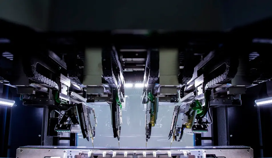
Phase 2: Post-Assembly Inspection – Catching Defects Early
Once components are mounted, the board becomes a Printed Circuit Board Assembly (PCBA). Inspection at this stage is critical for identifying issues related to the soldering and component placement process. The market for inspection equipment has grown rapidly, with projections showing a rise from $3.99 billion in 2024 to $4.43 billion in 2025, highlighting its importance.
Automated Optical Inspection (AOI) for Printed Circuit Board Assemblies (PCBAs)
After component placement, AOI is used again, but this time its focus shifts. The system checks for correct component placement, orientation, polarity, and soldering quality. It can identify missing components, incorrect parts, and visible solder joint defects like bridging or insufficient solder, catching the most common assembly errors quickly.
Solder Paste Inspection (SPI)
Before components are placed, a 3D SPI system measures the volume, alignment, and height of solder paste deposits on the pads. Since most soldering defects originate from improper solder paste application, this proactive check is one of the most effective ways to improve yields and prevent rework later.
X-Ray Inspection: Seeing Beyond the Surface
For components with connections hidden underneath the package, like Ball Grid Arrays (BGAs), an X-ray inspection is essential. It allows technicians to see through the component to inspect for solder voids, shorts, and proper ball alignment—defects that are impossible for optical inspections to detect. Advanced testing like this contributes to achieving defect failure rates as low as 1.2%.
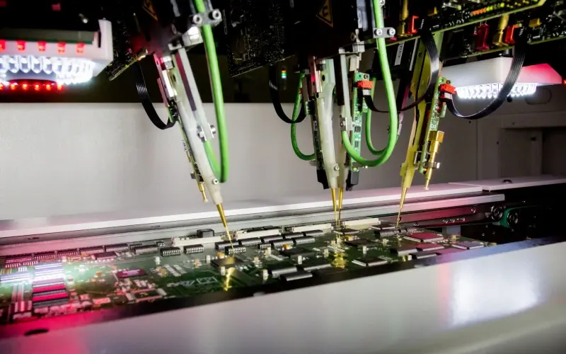
Phase 3: Electrical Testing – Validating Connectivity and Component Function
With the PCBA visually inspected, the next phase is to power it up and test its electrical characteristics. This stage confirms that all components are correctly connected and functioning at a basic level.
In-Circuit Test (ICT): The “Bed-of-Nails” Approach
ICT is a powerful testing method used for high-volume production. A custom fixture, known as a “bed-of-nails,” makes contact with numerous test points on the board simultaneously. It can quickly check for shorts, opens, and the values of passive components (resistors, capacitors), and verify the functionality of analog and digital components.
Flying Probe Testing: Flexibility for Lower Volumes and Prototypes
For prototypes and smaller production runs, a Flying Probe tester offers a fixtureless alternative to ICT. Robotic probes move around the board, making contact with component pins and vias to perform similar electrical measurements. While slower than ICT, it is highly flexible and cost-effective for low-volume scenarios as it requires no custom fixture.
Boundary Scan (JTAG/IEEE 1149.1): Testing Complex Digital Circuits
For modern, high-density boards with complex integrated circuits (ICs), physical access to all pins is often impossible. Boundary Scan testing uses a dedicated test logic built into many ICs to verify connections between them without needing direct physical probes, making it invaluable for testing intricate digital logic.
Phase 4: Functional Testing – Confirming Overall Performance
This is the ultimate validation step. Functional testing (FCT) powers up the board and simulates its intended operational environment to confirm it behaves exactly as the designers intended.
Functional Test (FCT): Simulating Real-World Operation
During FCT, the PCBA is connected to a test fixture that provides power and simulates the inputs and outputs it would see in the final product. The test system applies the correct voltage and signals, then measures the outputs to verify the entire circuit board performs to its specified requirements.
Firmware Programming and Test
For many products, this is also the stage where firmware or software is loaded onto the board’s microcontrollers or processors. The functional test then often includes routines that verify the firmware has been loaded correctly and that the software can properly control the hardware components.
Phase 5: Reliability and Environmental Testing – Ensuring Long-Term Durability
For products that must operate in demanding conditions or have long service lives, additional testing is required to ensure long-term reliability.
Environmental Testing: Stressing the Limits
This involves placing the PCBA in an environmental chamber to subject it to cycles of extreme temperature, humidity, and vibration. This process, known as Highly Accelerated Life Test (HALT), is designed to induce failures and identify design or component weaknesses that could cause problems in the field.
Burn-In Test: Accelerating the Detection of Early Failures
A burn-in test involves running the PCBA, often at an elevated temperature and voltage, for an extended period (hours or even days). This process is designed to weed out “infant mortality”—components that are prone to failing early in their lifecycle.
Interconnect Stress Testing (IST)
IST focuses on the reliability of the vias and interconnects within the PCB’s layers. It repeatedly heats the board to induce mechanical stress, monitoring for any increase in resistance that would indicate a developing crack or failure in the internal copper connections.
EMC (Electromagnetic Compatibility) Testing
EMC testing ensures the circuit board does not emit excessive electromagnetic interference that could affect other devices and is not susceptible to interference from external sources. This is a critical regulatory requirement for many electronic products.
Phase 6: Advanced Analysis and Continuous Improvement – Driving Excellence
Top-tier PCB manufacturers use testing not just to filter out bad boards but to improve the entire manufacturing process.
Root Cause Analysis with Advanced Laboratory Techniques
When failures are detected, advanced techniques like cross-sectioning, micro-sectioning, and Scanning Electron Microscopy (SEM) are used to perform a deep dive and find the exact root cause. This feedback is crucial for refining production parameters.
Design for Testability (DFT) and Design for Manufacturing (DFM)
The best quality assurance starts at the design stage. DFT principles involve designing the board with testing in mind—for example, by including accessible test points. DFM ensures the design is optimized for a smooth and repeatable manufacturing process, inherently reducing the likelihood of defects.
Establishing Quality Gates and Adhering to Industry Standards
A robust quality management system involves establishing clear “quality gates” at each phase of manufacturing. A board cannot proceed to the next stage until it passes the required tests. Adherence to industry standards like IPC provides a framework for maintaining consistent, high-quality production.
Conclusion: Building a Robust PCB Quality Assurance Ecosystem
Ensuring the quality and reliability of Printed Circuit Boards is a complex but essential endeavor. It requires a strategic, multi-layered approach that begins with the bare board and extends through assembly, functional validation, and long-term reliability screening. From Automated Optical Inspection and X-ray analysis to Flying Probe and Functional Testing, each method plays a critical role in a comprehensive quality assurance ecosystem.
By integrating these essential PCB testing items, manufacturers can significantly improve yields, reduce costly rework, and prevent field failures. The key takeaway for designers and engineers is to view testing not as a final hurdle but as an integral part of the design and manufacturing process. Engaging with knowledgeable PCB manufacturers early and embracing principles like Design for Testability are the ultimate steps toward building reliable, high-performance electronics that meet the demands of today’s technology landscape.

