


Introduction
PCBA stands for Printed Circuit Board + Assembly. It refers to the full process where a bare PCB undergoes SMT (Surface Mount Technology) placement or through-hole (DIP) insertion, followed by complete assembly. In China, the term “PCBA” is commonly used, while in Europe and the United States, the standard notation is “PCB’A” with an apostrophe—this is the official conventional expression.
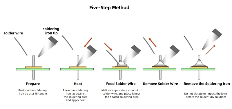
1. Five Steps for Manual PCBA Soldering
- Prepare: Position the soldering iron tip at a 45° angle relative to the solder joint.
- Heat: Touch the iron tip to the solder joint and apply heat evenly.
- Feed Solder Wire: Supply solder wire to the heated joint, allowing the solder to melt in the appropriate quantity.
- Remove Solder Wire: Once sufficient solder has melted and coated the joint, pull the solder wire away first.
- Remove the Iron: Avoid any vibration or impact on the joint before the solder fully solidifies. Then, carefully remove the soldering iron.
2. Fundamental Principles of PCBA Soldering
2.1 Surface Tension of the Board and Solder
The cohesion of tin-lead solder is extremely strong, causing molten solder to form a spherical shape. For a given volume, a sphere has the smallest surface area, which aligns with the low-energy state requirement. Flux functions similarly to a cleaner on oily metal surfaces. Additionally, surface tension is highly dependent on the cleanliness of the metal and its temperature. Ideal wetting (solder adhesion) occurs only when the wetting energy significantly exceeds the surface energy (cohesion) of the solder.
2.2 Formation of Intermetallic Compounds
Copper and tin form intermetallic grains during soldering. The shape and size of these grains are determined by the duration and intensity of heat applied to the joint. Lower heat input tends to produce a fine crystalline structure, which yields solder joints with optimal strength. Conversely, excessive heat or prolonged soldering time results in coarse, gritty, and brittle grains, leading to reduced shear strength of the joint.
2.3 Wetting Angle on the Board
When the board surface is heated to approximately 35°C above the solder’s eutectic point and a drop of solder is placed on the hot, fluxed surface, a meniscus (curved liquid surface) forms. The wetting ability of the metal can be partially evaluated by the shape of this meniscus:
- If the meniscus has a distinct undercut, resembles a water drop on an oily metal surface, or tends to be spherical, the metal is non-wettable.
- Good wetting is indicated by a small meniscus angle of less than 30°.
2.4 Wetting Action
Wetting refers to the process where hot liquid solder dissolves and spreads onto the metal surface to be joined. Solder and copper mix at the molecular level to form a new alloy phase (part copper, part solder). This process creates intermetallic bonds between the components, which is the core of high-quality soldering and determines the strength of the solder joint. For effective wetting:
- The copper surface must be clean and free of air-formed oxide layers.
- The solder and workpiece surface must reach the appropriate temperature.
2.5 Properties of Intermetallic Layers
PCBA uses copper as the base metal and tin-lead as the solder alloy. While lead does not form intermetallic compounds with copper, tin diffuses into copper, creating intermetallic compounds (Cu₃Sn and Cu₆Sn₅) at the solder-copper interface. Key characteristics:
- The intermetallic layer (composed of η phase and ε phase) must be extremely thin.
- In laser welding, the intermetallic layer thickness is on the order of 0.1 mm; in wave soldering and manual soldering, a high-quality joint typically has an intermetallic layer thickness exceeding 0.5 µm.
- Shear strength of the solder joint decreases as the intermetallic layer thickens. Thus, soldering time should be minimized to keep the layer thickness below 1 µm.
3. Precautions for Manual PCBA Soldering
3.1 Electrostatic Discharge (ESD) Control
Always wear an ESD wrist strap. The human body can accumulate over 10,000 volts of static electricity, while many ICs (Integrated Circuits) can be damaged by voltages exceeding 300 V. The wrist strap ensures static discharge to the ground, protecting sensitive components.
3.2 Handling the PCB and Components
- Wear gloves or finger cots; do not touch the PCB or component gold fingers with bare hands (oils and moisture from skin can cause contamination or corrosion).
- Hold the PCB only by its edges to avoid damaging components or solder joints on the board.
3.3 Soldering Parameters and Technique
- Use the correct soldering temperature, iron angle, and soldering sequence; maintain an appropriate soldering time.
- Prefer low-temperature soldering when possible: High temperatures accelerate iron tip oxidation—at 470°C, the oxidation rate is twice that at 380°C, significantly shortening the tip’s lifespan.
- Do not apply excessive pressure: Overpressure can damage or deform the iron tip. Heat transfers effectively if the tip makes full contact with the solder joint. Select an iron tip size matching the solder pad for optimal heat conduction.
- Avoid hitting or swinging the iron tip: This can damage the heater core, cause solder splatter (which may create short circuits on the PCB), and reduce the core’s lifespan.
3.4 Iron Tip Maintenance
- Clean the iron tip with a damp sponge to remove oxide and excess solder. The sponge should be moist (not soaking wet or dry):
- Overly wet sponges cause sudden temperature drops (thermal shock), leading to cold solder joints or open circuits; water residue can also corrode the PCB or cause shorts.
- Dry sponges fail to remove oxide, resulting in poor tinning of the tip and subsequent soldering defects.
- Check the sponge’s moisture level regularly and clean out solder dross at least three times a day.
- Keep the iron tip tinned (coated with a thin layer of solder) to reduce oxidation and extend its service life.
3.5 Solder and Flux Usage
- Use the right amount of solder: Excess solder causes short circuits (bridging) or hides defects; insufficient solder results in weak joints and accelerated oxidation, leading to joint failure over time.
- Use the right amount of flux: Excess flux can corrode the PCBA and cause electrical leakage; insufficient flux fails to remove oxides or promote wetting.
- Reduce solder splash: Avoid melting solder wire directly on the hot iron tip (flux heats rapidly and splatters). Instead, feed the solder wire to the heated joint.
3.6 Avoiding Heat Damage
Do not allow the soldering iron to burn the plastic insulation of nearby wires or the surfaces of components—this is particularly critical for tightly packed or complex-shaped PCBs.
3.7 Post-Soldering Self-Inspection
After soldering, inspect each joint against the following checklist:
- a. Are there any missed solder joints?
- b. Are the solder joints smooth, full, and shiny?
- c. Is there residual flux around the joint?
- d. Are there any solder bridges (unintended connections between pads)?
- e. Have any pads lifted or torn off the PCB?
- f. Are there any cracks in the solder joints?
- g. Are any joints needle-shaped (pulled tips) or uneven?
3.8 Safety and Ventilation
- Wear a mask to avoid inhaling harmful fumes from solder and flux.
- Use an extraction fan or fume hood to maintain good ventilation at the soldering workstation.
4. Practical Work and Skill Improvement Tips
- Practice steady hand control and precise heat management.
- Match the iron tip size to the solder joint/pad size for efficient heat transfer.
- Adjust the soldering iron temperature based on the components and solder type (e.g., lower temperatures for heat-sensitive components).
- Select the appropriate flux type for the application (e.g., no-clean flux for PCB assemblies).
- Keep the work area clean and organized to prevent contamination or component damage.
- Train operators on standard procedures to avoid bad habits that compromise quality.
5. Summary: Key Rules to Follow
- Wear an ESD wrist strap and ground yourself to protect sensitive components.
- Use gloves or finger cots—never touch components or PCBs with bare hands.
- Maintain the correct soldering angle, temperature, sequence, and time.
- Hold the PCB by its edges to avoid damaging components.
- Prioritize low-temperature soldering when feasible.
- Do not press or bang the soldering iron; use the correct tip size.
- Clean the iron tip regularly with a properly moistened sponge.
- Use the right amount of solder and flux—avoid excess or insufficiency.
- Keep the iron tip tinned to reduce oxidation.
- Prevent solder splash by feeding solder to the joint (not the iron tip).
- Avoid heat damage to nearby wires and components.
- Inspect all joints post-soldering using the provided checklist.
- Use safety equipment (mask, fume extractor) for a healthy work environment.
- Invest in training and skill checks to continuously improve soldering quality.
Final Note
Manual PCBA soldering is a combination of skill and process control. High-quality solder joints rely on proper heat management, precise timing, appropriate flux selection, clean metal surfaces, and careful handling. By minimizing heat exposure to control intermetallic layer growth, preventing ESD damage, and following standard cleaning and inspection procedures, you can consistently produce strong, reliable solder joints and enhance overall product quality.

