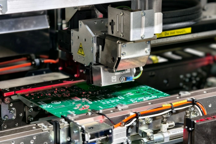

















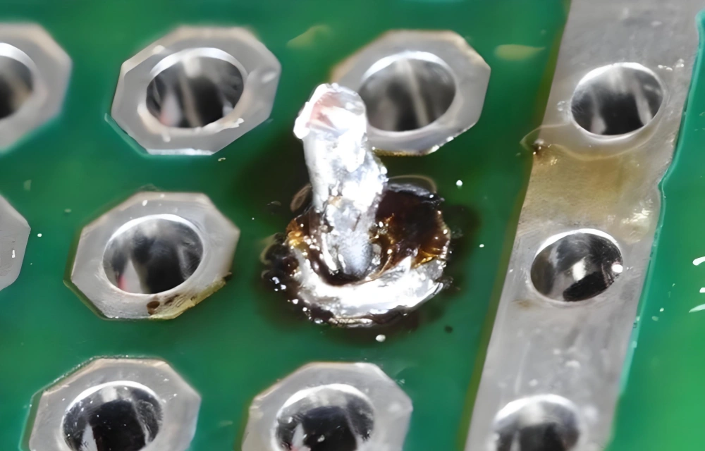
A PCB assembly defect is a condition in a populated board that does not meet its agreed workmanship, electrical, or functional requirements. Most PCB assembly defects result from a chain of small process variations rather than one isolated machine failure. Common sources include manufacturability issues in the design, inaccurate solder-paste printing, component or BOM errors, poor placement, an uncontrolled reflow profile, contamination, and inspection gaps. Prevent them by reviewing the design and BOM before build, controlling materials and process parameters, then verifying critical stages with SPI, AOI, X-ray, and electrical tests.
This guide maps the main failure modes to their causes, prevention methods, and the inspection method most likely to find them.
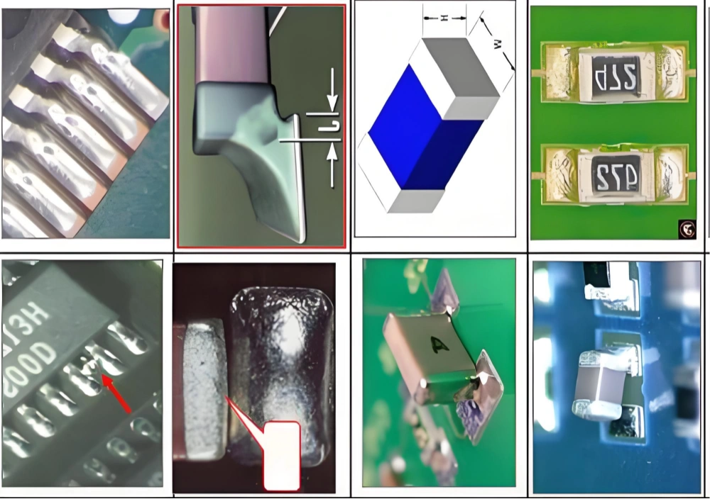
Common PCB assembly faults at a glance
The table below is a troubleshooting map, not a substitute for the acceptance criteria agreed with the customer. IPC-A-610 defines acceptability criteria for electronic assemblies, while J-STD-001 defines requirements for soldered electrical and electronic assemblies. Apply the current agreed revision, product class, and customer specification to each program.
| Defect | Typical causes | Prevention | Useful detection |
|---|---|---|---|
| Solder bridge or short | Excess paste, fine-pitch aperture, pad spacing, component shift, dirty stencil | Optimize aperture reduction, verify paste volume with SPI, maintain stencil cleanliness and placement accuracy | SPI, AOI, microscope, ICT |
| Insufficient solder or open joint | Low paste deposit, clogged aperture, oxidation, poor wetting, lifted lead | Control paste storage and print settings; verify pad finish and reflow wetting | SPI, AOI, continuity/ICT, X-ray for hidden joints |
| Tombstoning (drawbridge) | Unequal pad heating or paste volume, unbalanced pad geometry, component movement | Balance thermal mass, match aperture volumes, tune the profile and placement pressure | AOI and visual inspection |
| Component misalignment or rotation | Feeder/nozzle errors, wrong centroid data, board registration error, poor fiducials | Validate CAD-to-machine data, maintain feeders and fiducials, use first-article approval | AOI, vision inspection |
| Voids in BGA or thermal-pad solder | Trapped flux volatiles, unsuitable paste volume or apertures, unsuitable profile | Use window-pane apertures, appropriate paste and profile, and a voiding target agreed for the application | X-ray, cross-section when required |
| Solder balls or spatter | Excess paste, paste slumping, rapid ramp, moisture, dirty materials | Control paste rheology and storage, stencil design, ramp rate, and cleanliness | AOI, visual inspection |
| Head-in-pillow (BGA) | Warpage, oxidation, uneven paste, package and board movement during reflow | Manage moisture and warpage, use suitable paste volume and profile, verify BGA land design | X-ray screening; dye-and-pry or cross-section for confirmation |
| Non-wetting, lifted lead, or cold joint | Oxidized surfaces, insufficient heat, contamination, wrong alloy or profile | Confirm surface finish and material compatibility; profile the assembly and control handling | AOI, visual inspection, cross-section, electrical test |
| Wrong component or polarity | BOM revision error, counterfeit or mixed reels, feeder setup mistake, unclear marking | Lock approved BOM and AVL, barcode verification, kitting checks, polarity markings | Automated optical inspection, traceability review, functional test |
| Board warpage, delamination, or pad lifting | Moisture, excessive thermal stress, unsupported panel, unsuitable laminate or rework heat | Follow material handling rules, support the panel, control thermal cycles and rework temperatures | Visual inspection, dimensional checks, cross-section, functional test |
Where PCBA defects originate
1. Design, library, and BOM inputs
Many PCB assembly problems are created before manufacturing. A footprint with the wrong pad length, an aperture that does not match the pad, inadequate component-to-component clearance, or missing polarity information can produce a defect on every board. A BOM that allows substitutes without engineering approval can introduce a package, terminal finish, or moisture sensitivity level that the process was never qualified for.
Run a DFM/DFA review against the supplier’s rules. Check land patterns, clearances, fiducials, panel rails, test points, and polarized-part orientation. Philifast’s guide to DFT, DFM, and DFA design and its schematic-to-Gerber workflow cover this data handoff.
For procurement, freeze the approved manufacturer and part number in the BOM, record alternates explicitly, and require lot or date-code traceability for critical parts. Incoming inspection should verify part number, package, quantity, markings, and condition before kitting. A controlled electronic component sourcing process reduces wrong-part, counterfeit, and obsolete-component risk.
2. Solder-paste printing and stencil control
Printing determines how much solder is available before placement. Excess paste can bridge fine-pitch pads or create solder balls; too little paste can produce opens, weak joints, and head-in-pillow. Common contributors include worn or poorly cleaned stencils, blocked apertures, incorrect squeegee pressure or speed, board support problems, paste that has exceeded its working life, and poor alignment between stencil and PCB.
Use a printer setup that controls alignment, pressure, speed, separation, and underside cleaning. Segment large thermal-pad apertures and tune reductions for fine-pitch parts rather than applying one rule to the whole board. SPI should measure paste height, area, volume, and offset and feed trends back to the printer before defects reach reflow. Paste must be stored, tempered, mixed, and tracked according to its supplier instructions; do not treat a refrigerator temperature or open-time limit from one alloy as universal.
For process background, see Philifast’s PCB assembly overview, SMT assembly page, PCBA equipment guide, y reflow soldering guide.
3. Component placement and handling
Placement defects include offset, rotation, missing parts, wrong polarity, and wrong reference designators. Feeder setup, nozzle wear, vacuum loss, centroid data, fiducials, and board movement can contribute. Connectors and large packages may need a different strategy from small chip parts.
Prevent them with barcode-controlled kitting, feeder verification, first-article inspection, and locked programs. Keep moisture-sensitive devices within the supplier’s packaging and floor-life limits and follow applicable IPC/JEDEC J-STD-033 handling controls. Use ESD controls and record reel, lot, and machine data for traceability.
4. Reflow, wave, and selective soldering
The reflow profile must suit the alloy, board mass, component limits, and paste process window. Too little heat can leave non-wetting or cold joints; excessive peak temperature or time above liquidus can damage parts or laminate. Uneven heating can cause tombstoning or head-in-pillow, while poor support can warp thin or large panels.
Profile representative board locations, not just oven set points, and re-profile after material, panel, or oven changes. For mixed SMT/THT boards, confirm that wave or selective soldering does not disturb nearby joints. See the reflow versus wave soldering comparison.
Philifast — PCB Assembly & Manufacturing Services
One-stop PCBA workflow with DFM, SPI, AOI, and X-ray inspection to reduce defects and improve quality.
How to detect defects before shipment
No single inspection method sees every failure mode. A practical control plan uses several methods in sequence:
- SPI after printing measures paste volume and position. It catches a process drift while the board can still be cleaned and reprinted.
- AOI after reflow checks component presence, polarity, alignment, solder fillets, bridges, and many visible lead defects. AOI cannot reliably see hidden BGA joints or every underside condition.
- X-ray helps evaluate hidden joints, such as BGAs and bottom-terminated packages including QFNs, and is useful for assessing voiding. Conventional 2D X-ray alone may not prove head-in-pillow because it cannot always show whether the solder balls and paste fully coalesced. Set a voiding acceptance rule based on the package, thermal function, reliability requirement, and applicable standard; a single universal percentage is misleading.
- ICT and flying-probe tests check electrical nets, shorts, opens, and component values where test access and coverage are adequate. ICT is strongest when the design includes accessible test points and a stable fixture strategy.
- Pruebas funcionales (FCT) powers the product and verifies behavior. It can expose assembly errors that pass visual inspection, but it should not be used as the only quality gate because intermittent or latent solder defects may escape.
- Microscopy, cross-section, dye-and-pry, and failure analysis are used for containment and root-cause confirmation, not routine screening of every board.
En PCBA testing process guide provides more detail on combining these methods. Link results to the board serial number, program revision, material lots, and rework history.
A prevention workflow for PCB assembly quality
Use the following sequence when launching or improving a product:
- Review the package: release controlled Gerbers, pick-and-place data, drawings, BOM, approved alternates, and acceptance criteria. Run DFM/DFA before ordering stencils or parts.
- Qualify materials: verify PCB finish, solder paste alloy, component authenticity, moisture sensitivity, shelf life, and storage records. Define what happens when a substitute is proposed.
- Prove the setup: inspect the first panel, confirm feeder and polarity setup, measure SPI, capture the reflow profile, and approve AOI libraries before volume production.
- Control the line: trend SPI and AOI results, clean the stencil at a defined interval, verify ESD and humidity controls, and stop the line when a trend exceeds the agreed limit rather than sorting defects indefinitely.
- Test and learn: use electrical and functional tests appropriate to the product risk. For every recurring defect, contain affected lots, identify the escape point, verify the physical cause, and document a corrective action.
For a new design, prototype PCB assembly support can expose manufacturability issues early.
Philifast — PCB Assembly Quality Control
Comprehensive PCBA testing and inspection services to detect defects before shipment.
A practical troubleshooting method
When a defect appears, record the reference designator, board side, panel position, component lot, machine program, stencil ID, paste lot, and oven profile. Ask: Is it random or location-specific? Did it start after a material or setup change? Which inspection stage first found it?
A repeated footprint defect points to design, stencil, library, or thermal-balance issues. A defect that follows a reel or feeder points to material or placement control. A panel-wide shift suggests registration, support, or profile problems. Verify the cause with a controlled trial and update the process plan; do not mask it with manual rework.
PREGUNTAS FRECUENTES
What is the most common cause of PCB assembly defects?
There is no universal cause. Solder-paste printing and placement are frequent sources because small changes affect many joints, but design data, component condition, and reflow control can be equally important.
Can AOI find every PCBA defect?
No. AOI checks visible presence, polarity, alignment, bridges, and lead soldering, but not hidden BGA/QFN joints or electrical performance. Combine it with SPI, X-ray where needed, ICT or flying-probe, and functional testing.
Can X-ray confirm a head-in-pillow defect?
Not always. X-ray can screen BGA joint geometry and reveal voiding, but a conventional 2D image may not show whether the solder ball and paste fully joined. If head-in-pillow is suspected, use X-ray alongside process data and, when confirmation is necessary, a suitable destructive method such as dye-and-pry or cross-section analysis.
Why do components tombstone during reflow?
Tombstoning occurs when unequal forces lift one end of a small component. Pad heating or paste-volume imbalance and placement offset are common contributors. Balance the footprint and deposits, improve thermal uniformity, and verify the profile with thermocouples.
What causes BGA solder voids?
BGA voids form when flux volatiles are trapped as solder reflows. Paste formulation, aperture design and deposited volume, pad finish, package geometry, and the thermal profile can all affect their size and distribution. Evaluate voiding by its location and the product’s thermal and reliability needs, rather than applying one limit to every package.
How can procurement teams reduce PCB assembly problems?
Control the BOM and approved vendor list, require traceable parts, define substitution approval, and share the complete data package before quoting. Ask about incoming inspection, moisture-sensitive devices, ESD, stencil revision, test coverage, and nonconforming material.
What is the difference between a PCB defect and a PCBA defect?
A PCB defect is a problem in the bare board, such as an open trace, plating issue, or dimensional error. A PCBA defect is introduced during component assembly or soldering, such as a bridge, missing part, wrong polarity, or defective solder joint. Some failures interact: a poor pad finish on the bare PCB can become a non-wetting assembly defect.
Which standards should define acceptance?
Use the requirements named in the purchase order, drawings, and quality plan. Commercial programs commonly use IPC-A-610 for assembly acceptability and J-STD-001 for soldering requirements. NASA-STD-8739.3 covers soldered electrical connections for NASA programs and applies only when a program or contract invokes it. Agree the class, revision, inspection method, and evidence requirements before production.
Philifast — Reduce PCB Assembly Defects
From DFM review to final inspection, we help you build reliable boards.
Technical references
- IPC – publisher of IPC-A-610 and J-STD-001 for electronic assemblies.
- NASA Technical Standards System – source for NASA-STD-8739.3 and other NASA workmanship standards.
- JEDEC standards – semiconductor packaging and handling standards; IPC/JEDEC J-STD-033 addresses moisture-sensitive-device handling.
- NIST Advanced Manufacturing – research and measurement guidance relevant to manufacturing process control.
Published by Philifast Editorial Team · 2026-08-21